- 您現在的位置:買賣IC網 > PDF目錄373931 > AD8036 (Analog Devices, Inc.) Low Distortion, Wide Bandwidth Voltage Feedback Clamp Amps(低失真,寬帶電壓反饋鉗位放大器) PDF資料下載
參數資料
| 型號: | AD8036 |
| 廠商: | Analog Devices, Inc. |
| 英文描述: | Low Distortion, Wide Bandwidth Voltage Feedback Clamp Amps(低失真,寬帶電壓反饋鉗位放大器) |
| 中文描述: | 低失真,寬帶電壓反饋鉗放大器(低失真,寬帶電壓反饋鉗位放大器) |
| 文件頁數: | 20/24頁 |
| 文件大小: | 585K |
| 代理商: | AD8036 |
REV. 0
–20–
AD8036/AD8037
500mV
20ns
500mV
90
100
0%
10
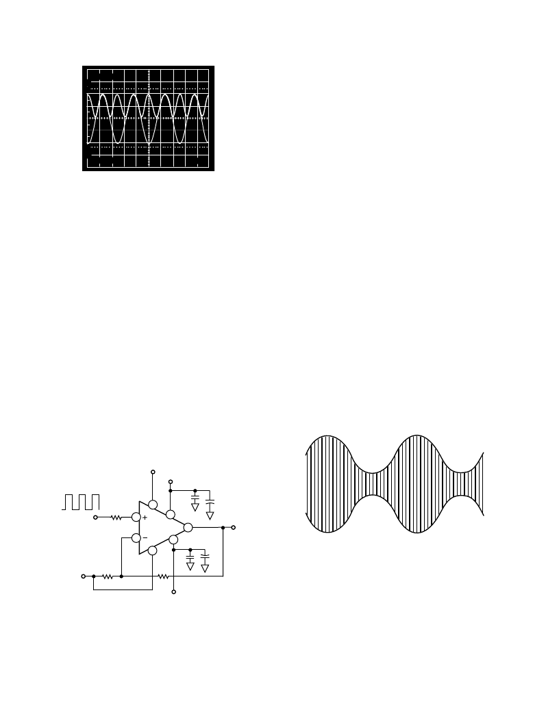
Figure 80. Full-Wave Rectifier Scope
Thus for either positive or negative input signals, the output is
unity times the absolute value of the input signal. The circuit
can be easily configured to produce the negative absolute value
of the input by applying the input to V
H
instead of V
L
.
The circuit can get to within about 40 mV of ground during the
time when the input crosses zero. This voltage is fixed over a
wide frequency range and is a result of the switching between
the conventional op amp input and the clamp input. But be-
cause there are no diodes to rapidly switch from forward to re-
verse bias, the performance far exceeds that of diode based full
wave rectifiers.
The 40 mV offset mentioned can be removed by adding an off-
set to the circuit. A 27.4 k
input resistor to the inverting input
will have a gain of 0.01, while changing the gain of the circuit by
only 1%. A plus or minus 4 V dc level (depending on the polar-
ity of the rectifier) into this resistor will compensate for the
offset.
Full wave rectifiers are useful in many applications including
AM signal detection, high frequency ac voltmeters and various
arithmetic operations.
Amplitude Modulator
In addition to being able to be configured as an amplitude de-
modulator (AM detector), the AD8037 can also be configured
as an amplitude modulator as shown in Figure 81.
+5V
CARRIER IN
100
10μF
AD8037
3
6
7
4
8
5
–5V
V
H
+
10
μF
+
274
V
L
2
V
H
AMPLITUDE MODULATOR
0.1μF
R
F
R
G
274
AM OUT
MODULATION IN
0.1
μF
Figure 81. Amplitude Modulator
The positive input of the AD8037 is driven with a square wave
of sufficient amplitude to produce clamping action at both the
high and low levels. This is the higher frequency carrier signal.
The modulation signal is applied to both the input of a unity
gain inverting amplifier and to V
L
, the lower clamping input.
V
H
is biased at +0.5 V dc.
To understand the circuit operation, it is helpful to first con-
sider a simpler circuit. If both V
L
and
V
H
were dc biased at
–0.5 V and the carrier and modulation inputs driven as above,
the output would be a 2 V p-p square wave at the carrier fre-
quency riding on a waveform at the modulating frequency. The
inverting input (modulation signal) is creating a varying offset to
the 2 V p-p square wave at the output. Both the high and low
levels clamp at twice the input levels on the clamps because the
noise gain of the circuit is two.
When V
L
is driven by the modulation signal instead of being
held at a dc level, a more complicated situation results. The re-
sulting waveform is composed of an upper envelope and a lower
envelope with the carrier square wave in between. The upper
and lower envelope waveforms are 180
°
out of phase as in a
typical AM waveform.
The upper envelope is produced by the upper clamp level being
offset by the waveform applied to the inverting input. This offset
is the opposite polarity of the input waveform because of the
inverting configuration.
The lower envelope is produced by the sum of two effects. First,
it is offset by the waveform applied to the inverting input as in
the case of the simplified circuit above. The polarity of this off-
set is in the same direction as the upper envelope. Second, the
output is driven in the opposite direction of the offset at twice
the offset voltage by the modulation signal being applied to V
L
.
This results from the noise gain being equal to two, and since
there is no inversion in this connection, it is opposite polarity
from the offset.
The result at the output for the lower envelope is the sum of
these two effects, which produces the lower envelope of an am-
plitude modulated waveform. See Figure 82.
AM WAVEFORM
Figure 82. AM Waveform
The depth of modulation can be modified in this circuit by
changing the amplitude of the modulation signal. This changes
the amplitude of the upper and lower envelope waveforms.
The modulation depth can also be changed by changing the dc
bias applied to V
H
. In this case the amplitudes of the upper and
lower envelope waveforms stay constant, but the spacing be-
tween them changes. This alters the ratio of the envelope ampli-
tude to the amplitude of the overall waveform.
相關PDF資料 |
PDF描述 |
|---|---|
| AD8037 | Low Distortion, Wide Bandwidth Voltage Feedback Clamp Amps(低失真,寬帶電壓反饋鉗位放大器) |
| AD8037AR-REEL7 | Low Distortion, Wide Bandwidth Voltage Feedback Clamp Amps |
| AD8036-EB | Low Distortion, Wide Bandwidth Voltage Feedback Clamp Amps |
| AD8037ACHIPS | Connector assemblies, Test RoHS Compliant: Yes |
| AD8037AN | Low Distortion, Wide Bandwidth Voltage Feedback Clamp Amps |
相關代理商/技術參數 |
參數描述 |
|---|---|
| AD8036_2000 | 制造商:AD 制造商全稱:Analog Devices 功能描述:Low Distortion, Wide Bandwidth Voltage Feedback Clamp Amps |
| AD8036ACHIPS | 制造商:AD 制造商全稱:Analog Devices 功能描述:Low Distortion, Wide Bandwidth Voltage Feedback Clamp Amps |
| AD8036AN | 功能描述:IC OPAMP VF ULDIST LN 70MA 8DIP RoHS:否 類別:集成電路 (IC) >> Linear - Amplifiers - Instrumentation 系列:CLAMPIN™ 標準包裝:2,500 系列:Excalibur™ 放大器類型:J-FET 電路數:1 輸出類型:- 轉換速率:45 V/µs 增益帶寬積:10MHz -3db帶寬:- 電流 - 輸入偏壓:20pA 電壓 - 輸入偏移:490µV 電流 - 電源:1.7mA 電流 - 輸出 / 通道:48mA 電壓 - 電源,單路/雙路(±):4.5 V ~ 38 V,±2.25 V ~ 19 V 工作溫度:-40°C ~ 85°C 安裝類型:表面貼裝 封裝/外殼:8-SOIC(0.154",3.90mm 寬) 供應商設備封裝:8-SOIC 包裝:帶卷 (TR) |
| AD8036ANZ | 功能描述:IC OPAMP VF ULDIST LN 70MA 8DIP RoHS:是 類別:集成電路 (IC) >> Linear - Amplifiers - Instrumentation 系列:CLAMPIN™ 標準包裝:1 系列:- 放大器類型:通用 電路數:4 輸出類型:滿擺幅 轉換速率:0.028 V/µs 增益帶寬積:105kHz -3db帶寬:- 電流 - 輸入偏壓:3nA 電壓 - 輸入偏移:100µV 電流 - 電源:3.3µA 電流 - 輸出 / 通道:12mA 電壓 - 電源,單路/雙路(±):2.7 V ~ 12 V,±1.35 V ~ 6 V 工作溫度:-40°C ~ 85°C 安裝類型:表面貼裝 封裝/外殼:14-TSSOP(0.173",4.40mm 寬) 供應商設備封裝:14-TSSOP 包裝:剪切帶 (CT) 其它名稱:OP481GRUZ-REELCT |
| AD8036AR | 功能描述:IC OPAMP VF ULDIST LN 70MA 8SOIC RoHS:否 類別:集成電路 (IC) >> Linear - Amplifiers - Instrumentation 系列:CLAMPIN™ 標準包裝:2,500 系列:Excalibur™ 放大器類型:J-FET 電路數:1 輸出類型:- 轉換速率:45 V/µs 增益帶寬積:10MHz -3db帶寬:- 電流 - 輸入偏壓:20pA 電壓 - 輸入偏移:490µV 電流 - 電源:1.7mA 電流 - 輸出 / 通道:48mA 電壓 - 電源,單路/雙路(±):4.5 V ~ 38 V,±2.25 V ~ 19 V 工作溫度:-40°C ~ 85°C 安裝類型:表面貼裝 封裝/外殼:8-SOIC(0.154",3.90mm 寬) 供應商設備封裝:8-SOIC 包裝:帶卷 (TR) |
發布緊急采購,3分鐘左右您將得到回復。