- 您現在的位置:買賣IC網 > PDF目錄373931 > AD8036AR (ANALOG DEVICES INC) Low Distortion, Wide Bandwidth Voltage Feedback Clamp Amps PDF資料下載
參數資料
| 型號: | AD8036AR |
| 廠商: | ANALOG DEVICES INC |
| 元件分類: | 運動控制電子 |
| 英文描述: | Low Distortion, Wide Bandwidth Voltage Feedback Clamp Amps |
| 中文描述: | OP-AMP, 11000 uV OFFSET-MAX, PDSO8 |
| 封裝: | SOIC-8 |
| 文件頁數: | 19/23頁 |
| 文件大小: | 387K |
| 代理商: | AD8036AR |
AD8036/AD8037
REV. A
–19–
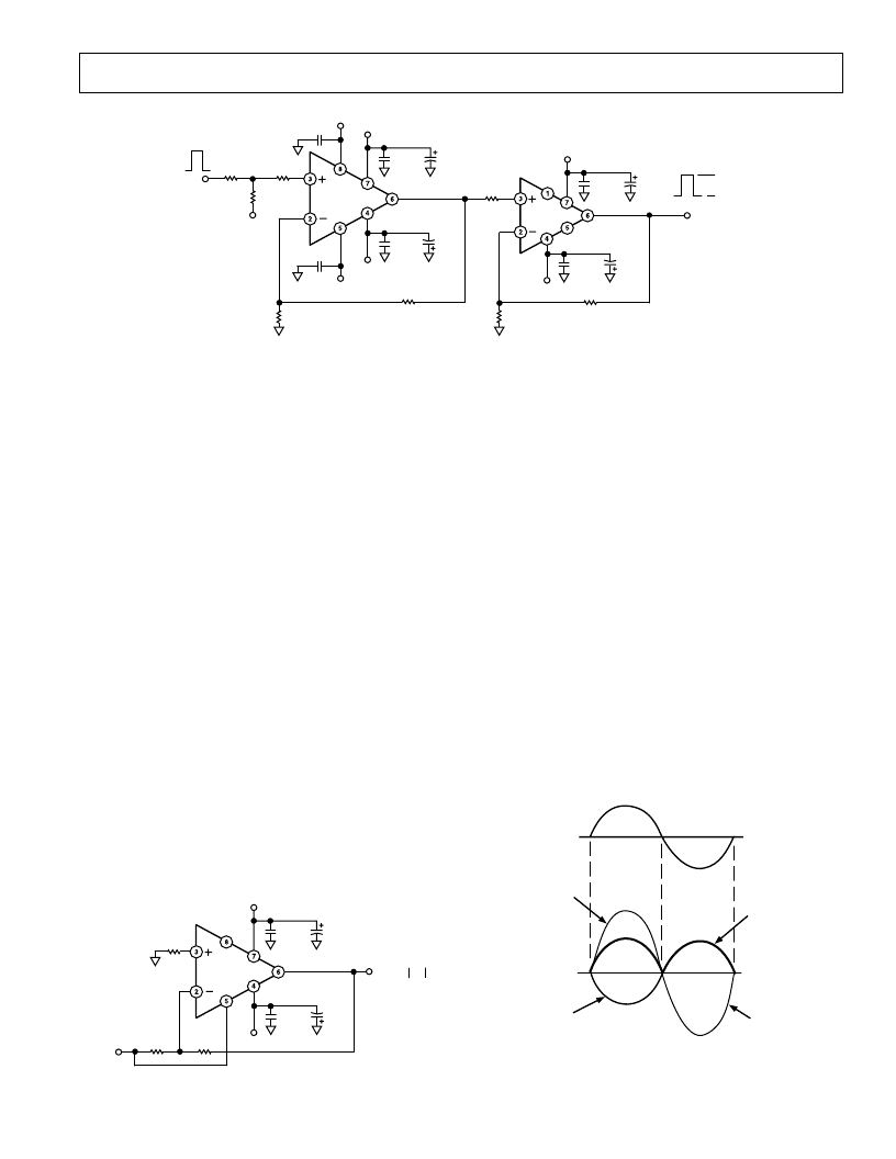
The circuit uses an AD8037 operating at a gain of two with an
AD811 to boost the output to the
±
12 V range. The AD811 was
chosen for its ability to operate with
±
15 V supplies and its high
slew rate.
R1 and R2 act as a level shifter to make the TTL signal levels be
approximately symmetrical above and below ground. This en-
sures that both the high and low logic levels will be clamped by
the AD8037. For well controlled signal levels in the output
pulse, the high and low output levels should result from the
clamping action of the AD8037 and not be controlled by either
the high or low logic levels passing through a linear amplifier.
For good rise and fall times at the output pulse, a logic family
with high speed edges should be used.
The high logic levels are clamped at two times the voltage at V
H
,
while the low logic levels are clamped at two times the voltage
at V
L
. The output of the AD8037 is amplified by the AD811
operating at a gain of 5. The overall gain of 10 will cause the
high output level to be 10 times the voltage at V
H
, and the low
output level to be 10 times the voltage at V
L
.
High Speed, Full-Wave Rectifier
The clamping inputs are additional inputs to the input stage of
the op amp. As such they have an input bandwidth comparable
to the amplifier inputs and lend themselves to some unique
functions when they are driven dynamically.
Figure 78 is a schematic for a full-wave rectifier, sometimes
called an absolute value generator. It works well up to 20 MHz
and can operate at significantly higher frequencies with some
degradation in performance. The distortion performance is sig-
nificantly better than diode based full-wave rectifiers, especially
at high frequencies.
V
OUT
=
V
IN
+5V
R
F
274
V
–5V
100
V
V
H
V
L
V
IN
0.1
m
F
10
m
F
AD8037
0.1
m
F
10
m
F
R
G
274
V
Figure 78. Full-Wave Rectifier
TTL
IN
+15V
PULSE
OUT
V
H
3
10
V
L
3
10
–15V
+5V
274
V
–5V
100
V
V
H
V
L
0.1
m
F
10
m
F
0.1
m
F
AD8037
0.1
m
F
10
m
F
V
H
0.1
m
F
V
L
274
V
1.3k
V
200
V
100
V
AD811
–15V
0.1
m
F
10
m
F
0.1
m
F
10
m
F
604
V
150
V
Figure 77. Programmable Pulse Generator
The circuit is configured as an inverting amplifier with a gain
of one. The input drives the inverting amplifier and also directly
drives V
L
, the lower level clamping input. The high level clamp-
ing input, V
H
, is left floating and plays no role in this circuit.
When the input is negative, the amplifier acts as a regular unity-
gain inverting amplifier and outputs a positive signal at the same
amplitude as the input with opposite polarity. V
L
is driven nega-
tive by the input, so it performs no clamping action, because the
positive output signal is always higher than the negative level
driving V
L
.
When the input is positive, the output result is the sum of two
separate effects. First, the inverting amplifier multiplies the in-
put by –1 because of its unity-gain inverting configuration. This
effectively produces an offset as explained above, but with a dy-
namic level that is equal to –1 times the input.
Second, although the positive input is grounded (through 100
),
the output is clamped at two times the voltage applied to V
L
(a
positive, dynamic voltage in this case). The factor of two is be-
cause the noise gain of the amplifier is two.
The sum of these two actions results in an output that is equal
to unity times the input signal for positive input signals, see Fig-
ure 79. For a input/output scope photo with an input signal of
20 MHz and amplitude
±
1 V, see Figure 80.
INPUT
FULL WAVE
RECTIFIED
OUTPUT
LOWER
CLAMPING
LEVEL WITH
NO NEG INPUT
OUTPUT
LOWER
CLAMPING
LEVEL
–1
3
INPUT
Figure 79.
相關PDF資料 |
PDF描述 |
|---|---|
| AD8037-EB | MB 26C 26#20 PIN PLUG |
| AD8036AR-REEL | Low Distortion, Wide Bandwidth Voltage Feedback Clamp Amps |
| AD8036AR-REEL7 | Low Distortion, Wide Bandwidth Voltage Feedback Clamp Amps |
| AD8037AR-REEL | Low Distortion, Wide Bandwidth Voltage Feedback Clamp Amps |
| AD803 | Clock Recovery and Data Retiming Phase-Locked Loop(時鐘恢復和重定時PLL) |
相關代理商/技術參數 |
參數描述 |
|---|---|
| AD8036AR-REEL | 制造商:Analog Devices 功能描述:OP Amp Single Volt Fdbk |
| AD8036AR-REEL7 | 功能描述:IC OPAMP VF ULDIST LN 70MA 8SOIC RoHS:否 類別:集成電路 (IC) >> Linear - Amplifiers - Instrumentation 系列:CLAMPIN™ 標準包裝:150 系列:- 放大器類型:音頻 電路數:2 輸出類型:- 轉換速率:5 V/µs 增益帶寬積:12MHz -3db帶寬:- 電流 - 輸入偏壓:100nA 電壓 - 輸入偏移:500µV 電流 - 電源:6mA 電流 - 輸出 / 通道:50mA 電壓 - 電源,單路/雙路(±):4 V ~ 32 V,±2 V ~ 16 V 工作溫度:-40°C ~ 85°C 安裝類型:表面貼裝 封裝/外殼:8-TSSOP(0.173",4.40mm 寬) 供應商設備封裝:8-TSSOP 包裝:管件 |
| AD8036ARZ | 功能描述:IC OPAMP VF ULDIST LN 70MA 8SOIC RoHS:是 類別:集成電路 (IC) >> Linear - Amplifiers - Instrumentation 系列:CLAMPIN™ 標準包裝:2,500 系列:- 放大器類型:通用 電路數:4 輸出類型:- 轉換速率:0.6 V/µs 增益帶寬積:1MHz -3db帶寬:- 電流 - 輸入偏壓:45nA 電壓 - 輸入偏移:2000µV 電流 - 電源:1.4mA 電流 - 輸出 / 通道:40mA 電壓 - 電源,單路/雙路(±):3 V ~ 32 V,±1.5 V ~ 16 V 工作溫度:0°C ~ 70°C 安裝類型:表面貼裝 封裝/外殼:14-TSSOP(0.173",4.40mm 寬) 供應商設備封裝:14-TSSOP 包裝:帶卷 (TR) 其它名稱:LM324ADTBR2G-NDLM324ADTBR2GOSTR |
| AD8036ARZ | 制造商:Analog Devices 功能描述:IC OP-AMP 240MHZ 1200V/ SOIC-8 |
| AD8036ARZ-REEL | 功能描述:IC OPAMP VF ULDIST LN 70MA 8SOIC RoHS:是 類別:集成電路 (IC) >> Linear - Amplifiers - Instrumentation 系列:CLAMPIN™ 標準包裝:150 系列:- 放大器類型:音頻 電路數:2 輸出類型:- 轉換速率:5 V/µs 增益帶寬積:12MHz -3db帶寬:- 電流 - 輸入偏壓:100nA 電壓 - 輸入偏移:500µV 電流 - 電源:6mA 電流 - 輸出 / 通道:50mA 電壓 - 電源,單路/雙路(±):4 V ~ 32 V,±2 V ~ 16 V 工作溫度:-40°C ~ 85°C 安裝類型:表面貼裝 封裝/外殼:8-TSSOP(0.173",4.40mm 寬) 供應商設備封裝:8-TSSOP 包裝:管件 |
發布緊急采購,3分鐘左右您將得到回復。