- 您現在的位置:買賣IC網 > PDF目錄373931 > AD803 (Analog Devices, Inc.) Clock Recovery and Data Retiming Phase-Locked Loop(時鐘恢復和重定時PLL) PDF資料下載
參數資料
| 型號: | AD803 |
| 廠商: | Analog Devices, Inc. |
| 英文描述: | Clock Recovery and Data Retiming Phase-Locked Loop(時鐘恢復和重定時PLL) |
| 中文描述: | 時鐘恢復和數據重定時鎖相環(時鐘恢復和重定時鎖相環) |
| 文件頁數: | 1/4頁 |
| 文件大小: | 129K |
| 代理商: | AD803 |
REV. 0
Information furnished by Analog Devices is believed to be accurate and
reliable. However, no responsibility is assumed by Analog Devices for its
use, nor for any infringements of patents or other rights of third parties
which may result from its use. No license is granted by implication or
otherwise under any patent or patent rights of Analog Devices.
a
AD803
One Technology Way, P.O. Box 9106, Norwood, MA 02062-9106, U.S.A.
Tel: 617/329-4700
World Wide Web Site: http://www.analog.com
Fax: 617/326-8703
Analog Devices, Inc., 1997
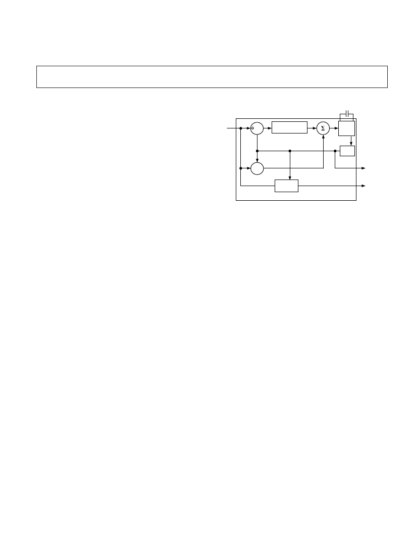
Clock Recovery and Data Retiming
Phase-Locked Loop
FUNCTIONAL BLOCK DIAGRAM
DATA
INPUT
DET
COMPENSATING
ZERO
LOOP
FILTER
VCO
RECOVERED
CLOCK
OUTPUT
AD803
C
D
F
DET
RETIMED
DATA
OUTPUT
RETIMING
DEVICE
PRODUCT DESCRIPTION
The AD803 employs a second order phase-locked loop architec-
ture to perform clock recovery and data retiming on Nonreturn
to Zero (NRZ) data. This architecture is capable of supporting
data rates between 18 Mbps and 30 Mbps. The product described
here is optimized for operation on 20.48 Mbps, a data rate used
in Passive Optical Networks (PONs).
Unlike other PLL-based clock recovery circuits, the AD803
does not require a preamble, an external VCXO, or an external
crystal to lock onto input data. The circuit acquires frequency
and phase lock using two control loops. The frequency acquisi-
tion loop initially acquires the clock frequency of the input data.
The phase-lock loop then acquires the phase of the input data,
and ensures that the phase of the output signals track changes in
the phase of the input data. The loop damping of the circuit is
dependent on the value of a user selected capacitor; this defines
jitter peaking performance and impacts acquisition time.
FEATURES
Standard Products: 20.48 Mbps
Accepts NRZ Data, No Preamble Required
Recovered Clock and Retimed Data Output
Phase-Locked Loop Type Clock Recovery—No Crystal
Required
Random Jitter: 3.0
8
rms
Pattern Jitter: Virtually Eliminated
Operating Temperature Range: –40
8
C to +85
8
C
Single Supply Operation: +5 V
TTL Compatible Inputs and Outputs
Low Power Consumption: 185 mW Typical, 275 mW
Maximum
The AD803 exhibits 0.08 dB jitter peaking, and acquires lock-
on random or scrambled data in 3
3
10
5
bit periods when using
a damping factor of 5.
The inclusion of a precisely trimmed VCO in the device elimi-
nates the need for external components for setting center fre-
quency, and the need for trimming of those components. The
VCO provides a clock output within
±
20% of its center fre-
quency in the absence of input data.
The AD803 exhibits virtually no pattern jitter due to the perfor-
mance of the patented phase detector. Loop jitter measures
3.0
°
rms. The nominal jitter bandwidth for the AD803 is set to
0.1% of the center frequency. The jitter bandwidth is mask
programmable.
The device operates from a single +5 V supply, and consumes
185 mW. The product accepts TTL level input signals, and
outputs TTL level signals that can drive a fan out of 10 ACT or
HCT CMOS inputs. The AD803 is specified to operate from
40
°
C to +85
°
C and is available in a 20-pin SOIC.
相關PDF資料 |
PDF描述 |
|---|---|
| AD8041AR-REEL | 160 MHz Rail-to-Rail Amplifier with Disable |
| AD8041 | 160 MHz Rail-to-Rail Amplifier with Disable |
| AD8041-EB | 160 MHz Rail-to-Rail Amplifier with Disable |
| AD8041AN | 160 MHz Rail-to-Rail Amplifier with Disable |
| AD8041AR | 160 MHz Rail-to-Rail Amplifier with Disable |
相關代理商/技術參數 |
參數描述 |
|---|---|
| AD8030 | 制造商:AD 制造商全稱:Analog Devices 功能描述:Low Power, High Speed Rail-to-Rail Input/Output Amplifier |
| AD80305BBCZ | 制造商:Analog Devices 功能描述:- Rail/Tube |
| AD80305XBCZ | 制造商:Analog Devices 功能描述:X-GRADE VERSION OF AD80305BBCZ, CATALINA RFIC, 1X1, 144CSBGA - Rail/Tube |
| AD8030AR | 功能描述:IC AMP GP R-R DUAL LP 8SOIC RoHS:否 類別:集成電路 (IC) >> Linear - Amplifiers - Instrumentation 系列:- 標準包裝:100 系列:- 放大器類型:通用 電路數:1 輸出類型:- 轉換速率:0.2 V/µs 增益帶寬積:- -3db帶寬:- 電流 - 輸入偏壓:100pA 電壓 - 輸入偏移:30µV 電流 - 電源:380µA 電流 - 輸出 / 通道:- 電壓 - 電源,單路/雙路(±):±2 V ~ 18 V 工作溫度:0°C ~ 70°C 安裝類型:表面貼裝 封裝/外殼:8-SOIC(0.154",3.90mm 寬) 供應商設備封裝:8-SO 包裝:管件 |
| AD8030AR | 制造商:Analog Devices 功能描述:AMP LOW POWER RRI/O 8030 SOIC8 |
發布緊急采購,3分鐘左右您將得到回復。