- 您現在的位置:買賣IC網 > PDF目錄373934 > AD8072ARM (ANALOG DEVICES INC) Low Cost, Dual/Triple Video Amplifiers PDF資料下載
參數資料
| 型號: | AD8072ARM |
| 廠商: | ANALOG DEVICES INC |
| 元件分類: | 音頻/視頻放大 |
| 英文描述: | Low Cost, Dual/Triple Video Amplifiers |
| 中文描述: | 2 CHANNEL, VIDEO AMPLIFIER, PDSO8 |
| 封裝: | MICRO, SOIC-8 |
| 文件頁數: | 4/11頁 |
| 文件大小: | 167K |
| 代理商: | AD8072ARM |
REV. A
AD8072/AD8073
–4–
CAUTION
ESD (electrostatic discharge) sensitive device. Electrostatic charges as high as 4000 V readily
accumulate on the human body and test equipment and can discharge without detection.
Although the AD8072 and AD8073 feature proprietary ESD protection circuitry, permanent
damage may occur on devices subjected to high energy electrostatic discharges. Therefore, proper
ESD precautions are recommended to avoid performance degradation or loss of functionality.
ABSOLUTE MAXIMUM RATINGS
1
Supply Voltage . . . . . . . . . . . . . . . . . . . . . . . . . . . . . . . .13.2 V
Internal Power Dissipation
2
AD8072 8-Lead Plastic (N) . . . . . . . . . . . . . . . . . 1.3 Watts
AD8072 8-Lead Small Outline (SO-8) . . . . . . . . . 0.9 Watts
AD8072 8-Lead
μ
SOIC (RM) . . . . . . . . . . . . . . . 0.6 Watts
AD8073 14-Lead Plastic (N) . . . . . . . . . . . . . . . . 1.6 Watts
AD8073 14-Lead Small Outline (R) . . . . . . . . . . . 1.0 Watts
Input Voltage (Common Mode) . . . . . . . . . . . . . . . . . . . .
±
V
S
Differential Input Voltage . . . . . . . . . . . . . . . . . . . . .
±
1.25 V
Output Short Circuit Duration . . . . . . . . . . . . . . . . . . . . . . . .
Observe Power Derating Curves
Storage Temperature Range
N, R, RM Packages . . . . . . . . . . . . . . . . . –65
°
C to +125
°
C
Lead Temperature Range (Soldering 10 sec) . . . . . . . .+300
°
C
NOTES
1
Stresses above those listed under Absolute Maximum Ratings may cause perma-
nent damage to the device. This is a stress rating only; functional operation of the
device at these or any other conditions above those indicated in the operational
section of this specification is not implied. Exposure to absolute maximum rating
conditions for extended periods may affect device reliability.
2
Specification is for device in free air:
8-Lead Plastic Package:
θ
JA
= 90
°
C/W
8-Lead SOIC Package:
θ
JA
= 140
°
C/W
8-Lead
μ
SOIC Package:
θ
JA
= 214
°
C/W
14-Lead Plastic Package:
θ
JA
= 75
°
C/W
14-Lead SOIC Package:
θ
JA
= 120
°
C/W
ORDERING GUIDE
Temperature
Range
Package
Description
Package
Option
Model
AD8072ARM
AD8072ARM-REEL
AD8072ARM-REEL7 –40
°
C to +85
°
C 7" Reel 8-Lead
μ
SOIC
AD8072JN
0
°
C to +70
°
C
AD8072JR
0
°
C to +70
°
C
AD8072JR-REEL
0
°
C to +70
°
C
AD8072JR-REEL7
0
°
C to +70
°
C
AD8073JN
0
°
C to +70
°
C
AD8073JR
0
°
C to +70
°
C
AD8073JR-REEL
0
°
C to +70
°
C
AD8073JR-REEL7
0
°
C to +70
°
C
–40
°
C to +85
°
C 8-Lead
μ
SOIC
–40
°
C to +85
°
C 13" Reel 8-Lead
μ
SOIC RM-8
RM-8
RM-8
N-8
SO-8
SO-8
SO-8
N-14
8-Lead Plastic DIP
8-Lead SOIC
13" Reel 8-Lead SOIC
7" Reel 8-Lead SOIC
14-Lead Plastic DIP
14-Lead Narrow SOIC R-14
13" Reel 14-Lead SOIC R-14
7" Reel 14-Lead SOIC
R-14
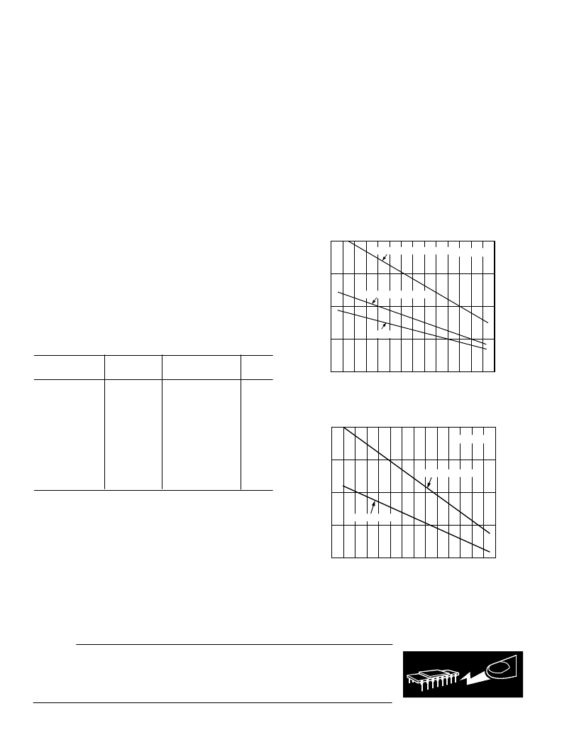
MAXIMUM POWER DISSIPATION
The maximum power that can be safely dissipated by the
AD8072 and AD8073 is limited by the associated rise in junc-
tion temperature. The maximum safe junction temperature for
plastic encapsulated devices is determined by the glass transition
temperature of the plastic, approximately +150
°
C. Exceeding
this limit temporarily may cause a shift in parametric perfor-
mance due to a change in the stresses exerted on the die by the
package. Exceeding a junction temperature of +175
°
C for an
extended period can result in device failure.
While the AD8072 and AD8073 are internally short circuit pro-
tected, this may not be sufficient to guarantee that the maximum
junction temperature (+150
°
C) is not exceeded under all condi-
tions. To ensure proper operation, it is necessary to observe the
maximum power derating curves shown in Figures 2 and 3.
M
–
AMBIENT TEMPERATURE
–
C
2.0
1.5
0
–
50
90
–
40
–
30
–
20
–
10
0
10
20
30
50 60
70
80
40
1.0
0.5
8-LEAD MINI-DIP PACKAGE
8-LEAD SOIC PACKAGE
T
J
= 150 C
SOIC
Figure 2. AD8072 Maximum Power Dissipation vs.
Temperature
AMBIENT TEMPERATURE
–
C
2.5
2.0
0.5
–
50
90
–
40
M
–
–
30
–
20
–
10 0
10 20
30 40 50
60
80
1.5
1.0
70
14-LEAD SOIC
14-LEAD DIP PACKAGE
T
J
= 150 C
Figure 3. AD8073 Maximum Power Dissipation vs.
Temperature
WARNING!
ESD SENSITIVE DEVICE
相關PDF資料 |
PDF描述 |
|---|---|
| AD8072ARM-REEL | Low Cost, Dual/Triple Video Amplifiers |
| AD8072ARM-REEL7 | Low Cost, Dual/Triple Video Amplifiers |
| AD8072JN | Low Cost, Dual/Triple Video Amplifiers |
| AD8072JR | Low Cost, Dual/Triple Video Amplifiers |
| AD8072JR-REEL | Low Cost, Dual/Triple Video Amplifiers |
相關代理商/技術參數 |
參數描述 |
|---|---|
| AD8072ARM-EBZ | 功能描述:BOARD EVAL FOR AD8072ARM RoHS:是 類別:編程器,開發系統 >> 評估演示板和套件 系列:* 標準包裝:1 系列:- 主要目的:電信,線路接口單元(LIU) 嵌入式:- 已用 IC / 零件:IDT82V2081 主要屬性:T1/J1/E1 LIU 次要屬性:- 已供物品:板,電源,線纜,CD 其它名稱:82EBV2081 |
| AD8072ARM-REEL | 制造商:Analog Devices 功能描述:OP Amp Dual Current Fdbk ±6V/12V 8-Pin MSOP T/R 制造商:Analog Devices 功能描述:OP AMP DUAL CURRENT FDBK 6V/12V 8MSOP - Tape and Reel 制造商:Rochester Electronics LLC 功能描述:USOIC LOW COST DUAL VIDEO AMPLIFIER - Tape and Reel |
| AD8072ARM-REEL7 | 制造商:Analog Devices 功能描述:OP Amp Dual Current Fdbk |
| AD8072ARMZ | 功能描述:IC OPAMP VIDEO DUAL 8MSOP RoHS:是 類別:集成電路 (IC) >> 線性 - 放大器 - 視頻放大器和頻緩沖器 系列:- 產品培訓模塊:Lead (SnPb) Finish for COTS Obsolescence Mitigation Program 標準包裝:50 系列:- 應用:TFT-LCD 面板:VCOM 驅動器 輸出類型:滿擺幅 電路數:1 -3db帶寬:35MHz 轉換速率:40 V/µs 電流 - 電源:3.7mA 電流 - 輸出 / 通道:1.3A 電壓 - 電源,單路/雙路(±):9 V ~ 20 V,±4.5 V ~ 10 V 安裝類型:表面貼裝 封裝/外殼:8-TSSOP,8-MSOP(0.118",3.00mm 寬)裸露焊盤 供應商設備封裝:8-uMax-EP 包裝:管件 |
| AD8072ARMZ-REEL | 功能描述:IC OPAMP VIDEO DUAL 8MSOP RoHS:是 類別:集成電路 (IC) >> 線性 - 放大器 - 視頻放大器和頻緩沖器 系列:- 標準包裝:1,000 系列:- 應用:驅動器 輸出類型:差分 電路數:3 -3db帶寬:350MHz 轉換速率:1000 V/µs 電流 - 電源:14.5mA 電流 - 輸出 / 通道:60mA 電壓 - 電源,單路/雙路(±):5 V ~ 12 V,±2.5 V ~ 6 V 安裝類型:表面貼裝 封裝/外殼:20-VFQFN 裸露焊盤 供應商設備封裝:20-QFN 裸露焊盤(4x4) 包裝:帶卷 (TR) |
發布緊急采購,3分鐘左右您將得到回復。