- 您現(xiàn)在的位置:買賣IC網(wǎng) > PDF目錄373938 > AD8133ACP-REEL7 (ANALOG DEVICES INC) Triple Differential Driver With Output Pull-Down PDF資料下載
參數(shù)資料
| 型號: | AD8133ACP-REEL7 |
| 廠商: | ANALOG DEVICES INC |
| 元件分類: | 通用總線功能 |
| 英文描述: | Triple Differential Driver With Output Pull-Down |
| 中文描述: | TRIPLE LINE DRIVER, QCC24 |
| 封裝: | 4 X 4 MM, MO-220VGGD-2, LFCSP-24 |
| 文件頁數(shù): | 5/16頁 |
| 文件大小: | 479K |
| 代理商: | AD8133ACP-REEL7 |
AD8133
ABSOLUTE MAXIMUM RATINGS
Table 3.
Parameter
Supply Voltage
All V
OCM
Power Dissipation
Input Common-Mode Voltage
Storage Temperature
Operating Temperature Range
Lead Temperature Range
(Soldering 10 sec)
Junction Temperature
Rev. 0 | Page 5 of 16
Rating
12 V
±V
S
See Figure 3
±V
S
65°C to +125°C
40°C to +85°C
300°C
150°C
Stresses above those listed under Absolute Maximum Ratings
may cause permanent damage to the device. This is a stress rat-
ing only and functional operation of the device at these or any
other conditions above those indicated in the operational sec-
tion of this specification is not implied. Exposure to absolute
maximum rating conditions for extended periods may affect
device reliability.
THERMAL RESISTANCE
θ
JA
is specified for the worst-case conditions, i.e., θ
JA
is specified
for the device soldered in a circuit board in still air.
Table 4. Thermal Resistance with the Underside Pad
Connected to the Plane
Package Type/PCB Type
θ
JA
24-Lead LFCSP/4-Layer
70
Unit
°C/W
Maximum Power Dissipation
The maximum safe power dissipation in the AD8133 package is
limited by the associated rise in junction temperature (T
J
) on
the die. At approximately 150°C, which is the glass transition
temperature, the plastic changes its properties. Even temporarily
exceeding this temperature limit may change the stresses that
the package exerts on the die, permanently shifting the para-
metric performance of the AD8133. Exceeding a junction tem-
perature of 175°C for an extended period of time can result in
changes in the silicon devices potentially causing failure.
The power dissipated in the package (P
D
) is the sum of the
quiescent power dissipation and the power dissipated in the
package due to the load drive for all outputs. The quiescent
power is the voltage between the supply pins (V
S
) times the
quiescent current (I
S
). The load current consists of differential
and common-mode currents flowing to the loads, as well as
currents flowing through the internal differential and common-
mode feedback loops. The internal resistor tap used in the
common-mode feedback loop places a 4 k differential load on
the output. RMS output voltages should be considered when
dealing with ac signals.
Airflow reduces θ
JA
. Also, more metal directly in contact with
the package leads from metal traces, through holes, ground,
and power planes reduces the θ
JA
. The exposed paddle on the
underside of the package must be soldered to a pad on the PCB
surface that is thermally connected to a copper plane in order to
achieve the specified θ
JA
.
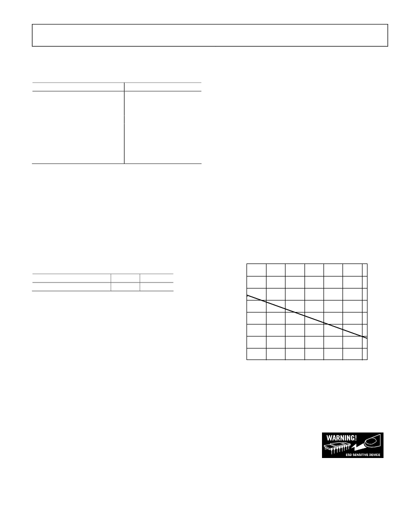
Figure 3 shows the maximum safe power dissipation in the
package versus ambient temperature for the 24-lead LFCSP
(70°C/W) package on a JEDEC standard 4-layer board with the
underside paddle soldered to a pad that is thermally connected
to a PCB plane. θ
JA
values are approximations.
0
–40
0.5
1.0
1.5
2.0
2.5
3.0
3.5
4.0
–20
0
20
40
60
80
0
AMBIENT TEMPERATURE (
°
C)
M
LFCSP
Figure 3. Maximum Power Dissipation vs. Temperature for a 4-Layer Board
ESD CAUTION
ESD (electrostatic discharge) sensitive device. Electrostatic charges as high as 4000 V readily accumulate on the
human body and test equipment and can discharge without detection. Although this product features proprie-
tary ESD protection circuitry, permanent damage may occur on devices subjected to high energy electrostatic
discharges. Therefore, proper ESD precautions are recommended to avoid performance degradation or loss of
functionality.
相關(guān)PDF資料 |
PDF描述 |
|---|---|
| AD8133ACPZ-REEL | Triple Differential Driver With Output Pull-Down |
| AD8133ACPZ-REEL7 | Triple Differential Driver With Output Pull-Down |
| AD8137 | Low Cost, Low Power 12-Bit Differential ADC Driver |
| AD8137YCP-R2 | Low Cost, Low Power 12-Bit Differential ADC Driver |
| AD8137YCP-REEL | Low Cost, Low Power 12-Bit Differential ADC Driver |
相關(guān)代理商/技術(shù)參數(shù) |
參數(shù)描述 |
|---|---|
| AD8133ACPZ-R2 | 制造商:Analog Devices 功能描述:SP Amp DIFF Line Driver Amp Triple ±6V/12V 24-Pin LFCSP EP T/R 制造商:Analog Devices 功能描述:SP AMP DIFF LINE DRVR AMP TRIPLE 6V/12V 24LFCSP EP - Tape and Reel 制造商:Rochester Electronics LLC 功能描述:- Bulk |
| AD8133ACPZ-REEL | 功能描述:IC OPAMP DIFF TRPL LDIST 24LFCSP RoHS:是 類別:集成電路 (IC) >> Linear - Amplifiers - Instrumentation 系列:- 標(biāo)準(zhǔn)包裝:100 系列:- 放大器類型:通用 電路數(shù):1 輸出類型:- 轉(zhuǎn)換速率:0.2 V/µs 增益帶寬積:- -3db帶寬:- 電流 - 輸入偏壓:100pA 電壓 - 輸入偏移:30µV 電流 - 電源:380µA 電流 - 輸出 / 通道:- 電壓 - 電源,單路/雙路(±):±2 V ~ 18 V 工作溫度:0°C ~ 70°C 安裝類型:表面貼裝 封裝/外殼:8-SOIC(0.154",3.90mm 寬) 供應(yīng)商設(shè)備封裝:8-SO 包裝:管件 |
| AD8133ACPZ-REEL7 | 功能描述:IC OPAMP DIFF TRPL LDIST 24LFCSP RoHS:是 類別:集成電路 (IC) >> Linear - Amplifiers - Instrumentation 系列:- 標(biāo)準(zhǔn)包裝:2,500 系列:- 放大器類型:通用 電路數(shù):2 輸出類型:滿擺幅 轉(zhuǎn)換速率:350 V/µs 增益帶寬積:180MHz -3db帶寬:320MHz 電流 - 輸入偏壓:12.5µA 電壓 - 輸入偏移:800µV 電流 - 電源:15mA 電流 - 輸出 / 通道:85mA 電壓 - 電源,單路/雙路(±):2.5 V ~ 12.6 V,±1.25 V ~ 6.3 V 工作溫度:-40°C ~ 85°C 安裝類型:表面貼裝 封裝/外殼:8-TSSOP,8-MSOP(0.118",3.00mm 寬) 供應(yīng)商設(shè)備封裝:8-MSOP 包裝:帶卷 (TR) |
| AD8134 | 制造商:AD 制造商全稱:Analog Devices 功能描述:Triple Differential Driver With Sync-On-Common-Mode |
| AD8134ACP-R2 | 制造商:Analog Devices 功能描述:SP Amp DIFF Line Driver Amp Triple 制造商:Analog Devices 功能描述:SP AMP DIFF LINE DRVR AMP TRIPLE 6V/6V 24LFCSP EP - Tape and Reel |
發(fā)布緊急采購,3分鐘左右您將得到回復(fù)。