- 您現在的位置:買賣IC網 > PDF目錄373939 > AD8148ACPZ-RL (Analog Devices, Inc.) Triple Differential Driver for Wideband Video PDF資料下載
參數資料
| 型號: | AD8148ACPZ-RL |
| 廠商: | Analog Devices, Inc. |
| 英文描述: | Triple Differential Driver for Wideband Video |
| 中文描述: | 三差分驅動器的寬帶視頻 |
| 文件頁數: | 14/24頁 |
| 文件大小: | 438K |
| 代理商: | AD8148ACPZ-RL |
AD8146/AD8147/AD8148
THEORY OF OPERATION
Each differential driver differs from a conventional op amp in
that it has two outputs whose voltages move in opposite directions.
Like an op amp, it relies on high open-loop gain and negative
feedback to force these outputs to the desired voltages. The
drivers make it easy to perform single-ended-to-differential
conversion, common-mode level shifting, and amplification of
differential signals.
Previous differential drivers, both discrete and integrated
designs, were based on using two independent amplifiers and
two independent feedback loops, one to control each of the
outputs. When these circuits are driven from a single-ended
source, the resulting outputs are typically not well balanced.
Achieving a balanced output has typically required exceptional
matching of the amplifiers and feedback networks.
DC common-mode level shifting has also been difficult with
previous differential drivers. Level shifting has required the use
of a third amplifier and feedback loop to control the output
common-mode level. Sometimes, the third amplifier was also
used to attempt to correct an inherently unbalanced circuit.
Excellent performance over a wide frequency range has proven
difficult with this approach.
Each of the drivers uses two feedback loops to separately
control the differential and common-mode output voltages.
The differential feedback, set by the internal resistors, controls
only the differential output voltage. The internal common-
mode feedback loop controls only the common-mode output
voltage. This architecture makes it easy to transmit signals over
the common-mode voltage channels by simply applying the
signal voltages to the V
OCM
inputs. The output common-mode
voltage is forced, by internal common-mode feedback, to equal
the voltage applied to the V
OCM
input, without affecting the
differential output voltage.
The driver architecture results in outputs that are highly
balanced over a wide frequency range without requiring
external components or adjustments. The common-mode
feedback loop forces the signal component of the output
common-mode voltage to be zeroed. The result is nearly
perfectly balanced differential outputs of identical
amplitude that are exactly 180° apart in phase.
DEFINITION OF TERMS
Differential Voltage
Differential voltage refers to the difference between two node
voltages that are balanced with respect to each other. For
example, in Figure 28 the output differential voltage (or
equivalently output differential mode voltage) is defined as
V
OUT, dm
= (
V
OP
V
ON
)
Rev. 0 | Page 14 of 24
Common-Mode Voltage
Common-mode voltage refers to the average of two node
voltages with respect to a common reference. The output
common-mode voltage is defined as
V
OUT, cm
= (
V
OP
+
V
ON
)/2
Output Balance
Output balance is a measure of how well the differential output
signals are matched in amplitude and how close they are to
exactly 180° apart in phase. Balance is most easily determined
by placing a well-matched resistor divider between the differential
output voltage nodes and comparing the magnitude of the signal at
the divider’s midpoint with the magnitude of the differential
signal. By this definition, output balance error is the magnitude
of the change in output common-mode voltage divided by the
magnitude of the change in output differential mode voltage in
response to a differential input signal.
dm
OUT
cm
OUT
V
V
Error
Balance
Output
,
,
Δ
Δ
=
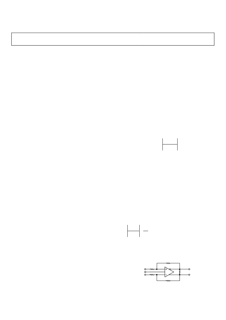
ANALYZING AN APPLICATION CIRCUIT
The drivers use high open-loop gain and negative feedback to
force their differential and common-mode output voltages to
minimize the differential and common-mode input error
voltages. The differential input error voltage is defined as the
voltage between the differential inputs labeled V
AP
and V
AN
in
Figure 28. For most purposes, this voltage can be assumed to be
zero. Similarly, the difference between the actual output common-
mode voltage and the voltage applied to V
OCM
can also be
assumed to be zero. Starting from these two assumptions,
any application circuit can be analyzed.
CLOSED-LOOP GAIN
The differential mode gain of the circuit in Figure 28 can be
described by
G
F
dm
IN,
dm
OUT,
V
R
R
V
=
where:
R
F
is 1.0 kΩ and R
G
is 500 Ω nominally for the AD8146 and
AD8147.
R
F
is 2.0 kΩ and R
G
is 500 Ω nominally for the AD8148.
R
G
V
AP
V
AN
V
IP
IN
+
V
IN, dm
–
V
OCM
V
ON
V
OUT, dm
V
OP
R
G
R
F
R
F
R
L, dm
0
Figure 28. Internal Architecture and Signal Name Definitions
相關PDF資料 |
PDF描述 |
|---|---|
| AD8150-EVAL | 33 x 17, 1.5 Gbps Digital Crosspoint Switch |
| AD8150 | 33 x 17, 1.5 Gbps Digital Crosspoint Switch |
| AD8150AST | 33 x 17, 1.5 Gbps Digital Crosspoint Switch |
| AD8151-EVAL | GPA/SK 300X280X1,5... |
| AD8151 | 33 x 17, 3.2 Gb/s Digital Crosspoint Switch |
相關代理商/技術參數 |
參數描述 |
|---|---|
| AD815 | 制造商:未知廠家 制造商全稱:未知廠家 功能描述:SILICON DUAL DIFFERNTIAL AMPLIFIER TRANSISTORS |
| AD815_05 | 制造商:AD 制造商全稱:Analog Devices 功能描述:High Output Current Differential Driver |
| AD8150 | 制造商:AD 制造商全稱:Analog Devices 功能描述:33 x 17, 1.5 Gbps Digital Crosspoint Switch |
| AD8150AST | 制造商:Rochester Electronics LLC 功能描述:LQFP 1.5GBPS 33X17 DIGITAL CROSSPOINT SW - Tape and Reel 制造商:Analog Devices 功能描述:IC SWITCH CROSSPOINT |
| AD8150ASTZ | 功能描述:IC CROSSPOINT SWIT 33X17 184LQFP RoHS:是 類別:集成電路 (IC) >> 接口 - 模擬開關,多路復用器,多路分解器 系列:XStream™ 應用說明:Ultrasound Imaging Systems Application Note 產品培訓模塊:Lead (SnPb) Finish for COTS Obsolescence Mitigation Program 標準包裝:250 系列:- 功能:開關 電路:單刀單擲 導通狀態電阻:48 歐姆 電壓電源:單電源 電壓 - 電源,單路/雙路(±):2.7 V ~ 5.5 V 電流 - 電源:5µA 工作溫度:0°C ~ 70°C 安裝類型:表面貼裝 封裝/外殼:48-LQFP 供應商設備封裝:48-LQFP(7x7) 包裝:托盤 |
發布緊急采購,3分鐘左右您將得到回復。