- 您現(xiàn)在的位置:買賣IC網(wǎng) > PDF目錄373939 > AD8148ACPZ-RL (Analog Devices, Inc.) Triple Differential Driver for Wideband Video PDF資料下載
參數(shù)資料
| 型號: | AD8148ACPZ-RL |
| 廠商: | Analog Devices, Inc. |
| 英文描述: | Triple Differential Driver for Wideband Video |
| 中文描述: | 三差分驅(qū)動器的寬帶視頻 |
| 文件頁數(shù): | 7/24頁 |
| 文件大小: | 438K |
| 代理商: | AD8148ACPZ-RL |
AD8146/AD8147/AD8148
ABSOLUTE MAXIMUM RATINGS
Rev. 0 | Page 7 of 24
Table 3.
Parameter
Supply Voltage
All V
OCM
Power Dissipation
Input Common-Mode Voltage
Storage Temperature Range
Operating Temperature Range
Lead Temperature (Soldering, 10 sec)
Junction Temperature
Rating
11 V
±V
S
See Figure 3
±V
S
65°C to +125°C
40°C to +85°C
300°C
150°C
Stresses above those listed under Absolute Maximum Ratings
may cause permanent damage to the device. This is a stress
rating only and functional operation of the device at these or
any other conditions above those indicated in the operational
section of this specification is not implied. Exposure to absolute
maximum rating conditions for extended periods may affect
device reliability.
THERMAL RESISTANCE
θ
JA
is specified for the worst-case conditions, that is, θ
JA
is
specified for the device soldered in a circuit board in still air.
Table 4. Thermal Resistance with the Underside Pad
Connected to the Plane
Package Type/PCB Type
24-Lead LFCSP/4-Layer
θ
JA
57
Unit
°C/W
Maximum Power Dissipation
The maximum safe power dissipation in the AD8146/
AD8147/AD8148 package is limited by the associated rise in
junction temperature (T
J
) on the die. At approximately 150°C,
which is the glass transition temperature, the plastic changes its
properties. Even temporarily exceeding this temperature limit
can change the stresses that the package exerts on the die,
permanently shifting the parametric performance of the
AD8146/AD8147/AD8148. Exceeding a junction temperature
of 175°C for an extended time can result in changes in the
silicon devices, potentially causing failure.
The power dissipated in the package (P
D
) is the sum of the
quiescent power dissipation and the power dissipated in the
package due to the load drive for all outputs. The quiescent
power is the voltage between the supply pins (V
S
) times the
quiescent current (I
S
). The load current consists of differential
and common-mode currents flowing to the loads, as well as
currents flowing through the internal differential and common-
mode feedback loops. The internal resistor tap used in the
common-mode feedback loop places a 4 kΩ differential load on
the output. Differential feedback, network resistor values are
given in the Theory of Operation section and Applications
section. RMS output voltages should be considered when
dealing with ac signals.
Airflow reduces θ
JA
. In addition, more metal directly in contact
with the package leads from metal traces, through holes,
ground, and power planes reduces the θ
JA
. The exposed paddle
on the underside of the package must be soldered to a pad on
the PCB surface that is thermally connected to a ground plane
to achieve the specified θ
JA
.
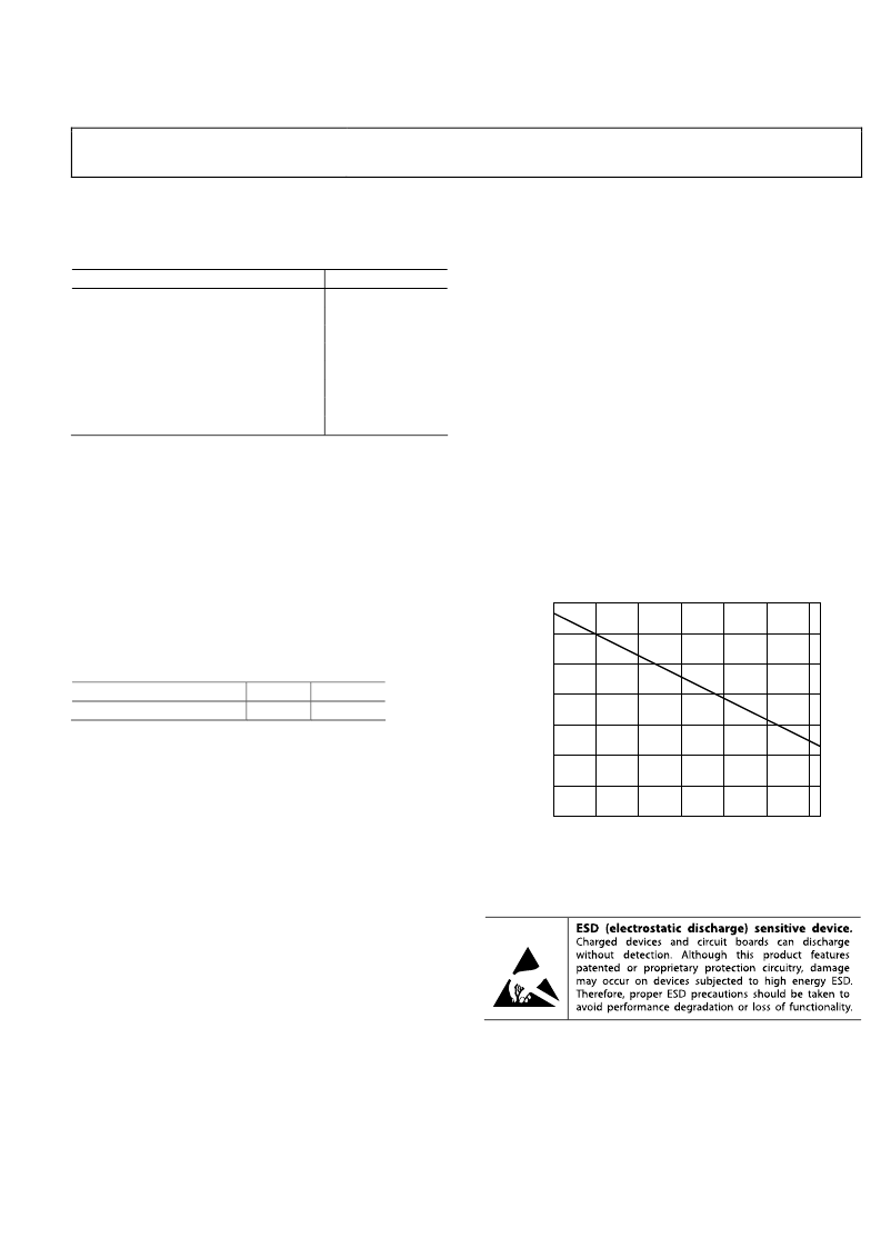
Figure 3 shows the maximum safe power dissipation in the
package vs. the ambient temperature for the 24-lead LFCSP
(57°C/W) package on a JEDEC standard 4-layer board with the
underside paddle soldered to a pad that is thermally connected
to a ground plane. θ
JA
values are approximations.
3.5
0
–40
–20
0
20
40
60
80
AMBIENT TEMPERATURE (°C)
M
3.0
2.5
2.0
1.5
1.0
0.5
0
Figure 3. Maximum Power Dissipation vs. Temperature for a 4-Layer Board
ESD CAUTION
相關(guān)PDF資料 |
PDF描述 |
|---|---|
| AD8150-EVAL | 33 x 17, 1.5 Gbps Digital Crosspoint Switch |
| AD8150 | 33 x 17, 1.5 Gbps Digital Crosspoint Switch |
| AD8150AST | 33 x 17, 1.5 Gbps Digital Crosspoint Switch |
| AD8151-EVAL | GPA/SK 300X280X1,5... |
| AD8151 | 33 x 17, 3.2 Gb/s Digital Crosspoint Switch |
相關(guān)代理商/技術(shù)參數(shù) |
參數(shù)描述 |
|---|---|
| AD815 | 制造商:未知廠家 制造商全稱:未知廠家 功能描述:SILICON DUAL DIFFERNTIAL AMPLIFIER TRANSISTORS |
| AD815_05 | 制造商:AD 制造商全稱:Analog Devices 功能描述:High Output Current Differential Driver |
| AD8150 | 制造商:AD 制造商全稱:Analog Devices 功能描述:33 x 17, 1.5 Gbps Digital Crosspoint Switch |
| AD8150AST | 制造商:Rochester Electronics LLC 功能描述:LQFP 1.5GBPS 33X17 DIGITAL CROSSPOINT SW - Tape and Reel 制造商:Analog Devices 功能描述:IC SWITCH CROSSPOINT |
| AD8150ASTZ | 功能描述:IC CROSSPOINT SWIT 33X17 184LQFP RoHS:是 類別:集成電路 (IC) >> 接口 - 模擬開關(guān),多路復(fù)用器,多路分解器 系列:XStream™ 應(yīng)用說明:Ultrasound Imaging Systems Application Note 產(chǎn)品培訓(xùn)模塊:Lead (SnPb) Finish for COTS Obsolescence Mitigation Program 標(biāo)準(zhǔn)包裝:250 系列:- 功能:開關(guān) 電路:單刀單擲 導(dǎo)通狀態(tài)電阻:48 歐姆 電壓電源:單電源 電壓 - 電源,單路/雙路(±):2.7 V ~ 5.5 V 電流 - 電源:5µA 工作溫度:0°C ~ 70°C 安裝類型:表面貼裝 封裝/外殼:48-LQFP 供應(yīng)商設(shè)備封裝:48-LQFP(7x7) 包裝:托盤 |
發(fā)布緊急采購,3分鐘左右您將得到回復(fù)。