- 您現(xiàn)在的位置:買賣IC網 > PDF目錄373939 > AD816 (Analog Devices, Inc.) 500 mA Differential Driver & Dual Low Noise (VF) Amplifiers(500mA差分驅動器和雙低噪電壓反饋放大器) PDF資料下載
參數(shù)資料
| 型號: | AD816 |
| 廠商: | Analog Devices, Inc. |
| 英文描述: | 500 mA Differential Driver & Dual Low Noise (VF) Amplifiers(500mA差分驅動器和雙低噪電壓反饋放大器) |
| 中文描述: | 500毫安差分驅動器 |
| 文件頁數(shù): | 12/16頁 |
| 文件大小: | 479K |
| 代理商: | AD816 |
AD816
REV. 0
–12–
PRINTED CIRCUIT BOARD LAYOUT
CONSIDERATIONS
As to be expected for a wideband amplifier, PC board parasitics
can affect the overall closed-loop performance. Of concern are
stray capacitances at the output and the inverting input nodes. If
a ground plane is to be used on the same side of the board as
the signal traces, a space (5 mm min) should be left around the
signal lines to minimize coupling.
POWER SUPPLY BYPASSING
Adequate power supply bypassing can be critical when
optimizing the performance of a high frequency circuit.
Inductance in the power supply leads can form resonant circuits
that produce peaking in the amplifier’s response. In addition, if
large current transients must be delivered to the load, then
bypass capacitors (typically greater than 1
μ
F) will be required
to provide the best settling time and lowest distortion. A parallel
combination of 10.0
μ
F and 0.1
μ
F is recommended. Under
some low frequency applications, a bypass capacitance of greater
than 10
μ
F may be necessary. Due to the large load currents
delivered by the AD816, special consideration must be given to
careful bypassing. The ground returns on both supply bypass
capacitors as well as signal common must be “star” connected
as shown in Figure 44.
R
F
R
G
(OPTIONAL)
R
F
+V
S
+OUT
–OUT
–V
S
+IN
–IN
DRIVER A
DRIVER B
R
F
R
G
R
F
R
G
IN
IN
RECEIVER A
RECEIVER B
OUT
OUT
Figure 44. Signal Ground Connected in “Star”
Configuration
POWER CONSIDERATIONS
The 500 mA drive capability of the AD816 driver enables it to
drive a 50
load at 40 V p-p when it is configured as a dif-
ferential driver. This implies a power dissipation, P
IN
, of nearly
5 watts. To ensure reliability, the junction temperature of the
AD816 should be maintained at less than 175
°
C. For this
reason, the AD816 will require some form of heat sinking in
most applications. The thermal diagram of Figure 45 gives the
basic relationship between junction temperature (T
J
) and
various components of
θ
JA
.
T
J
=
T
A
+
P
IN
θ
JA
Equation 1
θ
A
(JUNCTION TO
DIE MOUNT)
θ
B
(DIE MOUNT
TO CASE)
θ
A
+
θ
B
=
θ
JC
CASE
T
A
T
J
θ
JC
θ
CA
T
A
θ
JA
T
J
P
IN
WHERE:
P
IN
= DEVICE POWER DISSIPATION
T
A
= AMBIENT TEMPERATURE
T
J
= JUNCTION TEMPERATURE
θ
JC
= THERMAL RESISTANCE – JUNCTION TO CASE
θ
CA
= THERMAL RESISTANCE – CASE TO AMBIENT
Figure 45. A Breakdown of Various Package Thermal
Resistances
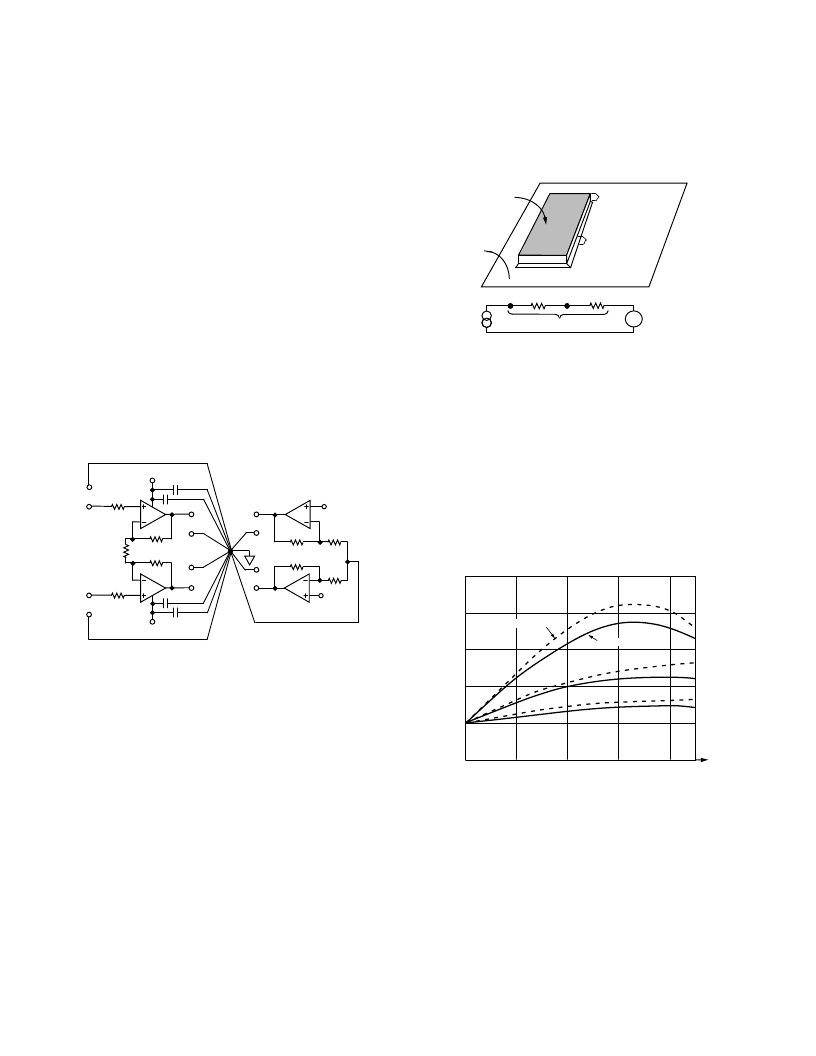
Figure 46 gives the relationship between output voltage swing
into various loads and the power dissipated by the AD816 (P
IN
).
This data is given for both sine wave and square wave (worst
case) conditions. It should be noted that these graphs are for
mostly resistive (phase <
±
10
°
) loads. When the power dissipation
requirements are known, Equation 1 and the graph on Figure 47
can be used to choose an appropriate heat sinking configuration.
4
3
P
I
10
20
V
OUT
– Volts p-p
30
40
2
1
R
L
= 50
V
R
L
= 100
V
R
L
= 200
V
f = 1kHz
V
S
=
±
15V
SQUARE WAVE
SINE WAVE
Figure 46. Total Power Dissipation vs Differential Driver
Output Voltage
相關PDF資料 |
PDF描述 |
|---|---|
| AD8170AN | 250 MHz, 10 ns Switching Multiplexers w/Amplifier |
| AD8170AR | 250 MHz, 10 ns Switching Multiplexers w/Amplifier |
| AD8170-EB | 250 MHz, 10 ns Switching Multiplexers w/Amplifier |
| AD8170AR-REEL | 250 MHz, 10 ns Switching Multiplexers w/Amplifier |
| AD8174-EB | 250 MHz, 10 ns Switching Multiplexers w/Amplifier |
相關代理商/技術參數(shù) |
參數(shù)描述 |
|---|---|
| AD816AVR | 制造商:Rochester Electronics LLC 功能描述:ADSL TRANSCEIVER - Bulk |
| AD816AY | 制造商:Rochester Electronics LLC 功能描述:ADSL TRANSCEIVER - Bulk |
| AD816AYR | 制造商:未知廠家 制造商全稱:未知廠家 功能描述:Analog IC |
| AD816AYS | 制造商:Rochester Electronics LLC 功能描述:- Bulk |
發(fā)布緊急采購,3分鐘左右您將得到回復。