- 您現(xiàn)在的位置:買賣IC網(wǎng) > PDF目錄373939 > AD816 (Analog Devices, Inc.) 500 mA Differential Driver & Dual Low Noise (VF) Amplifiers(500mA差分驅(qū)動(dòng)器和雙低噪電壓反饋放大器) PDF資料下載
參數(shù)資料
| 型號(hào): | AD816 |
| 廠商: | Analog Devices, Inc. |
| 英文描述: | 500 mA Differential Driver & Dual Low Noise (VF) Amplifiers(500mA差分驅(qū)動(dòng)器和雙低噪電壓反饋放大器) |
| 中文描述: | 500毫安差分驅(qū)動(dòng)器 |
| 文件頁數(shù): | 15/16頁 |
| 文件大小: | 479K |
| 代理商: | AD816 |
AD816
REV. 0
–15–
by R101 and all the downstream circuitry comprised of T1, the
transmission line and its termination. For an ideal transformer,
transmission line and termination, this will appear to be 15
,
and thus the signal appearing at Pins 1 and 2 of T1 will be the
output of D1 divided by two in the ideal case. This signal is
applied to the input of R1 (Receive 1 of the AD816) (Pin 3) via
R105.
In some ADSL systems (DMT), there is a need to transmit
higher crest factor signals. Typically this is done by increasing
the turns ratio of T1 to as much as 4:1. In this case, R101 and
R201 would be 3.75
, and the peak current of the AD816
(1 A) would be the drive limit of the transmitter.
R1 is configured as a difference amplifier. The negative side
(Pin 2) is driven by another signal that is a divided down version
of the output of D1. This circuit is formed by R102 as one side
of the voltage divider along with R103, C101, R104 and L101
as the other half of the divider. If the frequency dependent
impedance part of this circuit matches the transformer, trans-
mission line and termination impedance, then the signals
applied to both sides of the difference-amp-configured R1 will
be the same, and the transmit signal will be totally subtracted
out by the circuit.
In a real-world situation, it is not practical (or even possible) to
subtract out all of the transmit signal (100% trans-hybrid loss),
but only provide a first order cancellation which goes a long way
toward reducing the dynamic range of the RCVOUT signal.
The overall performance of this circuit depends on the ability to
build a lumped element network that matches the impedance of
the transmission line over the frequency range required for
ADSL (
≈
20 kHz to 1.1 MHz).
The circuits formed by D2 and R2 of the AD816 are totally
symmetric with those formed by D1 and R1 and work in the
same fashion. All the components in the D1, R1 circuits that are
numbered with 100 range numbers are numbered with 200
range numbers in the D2, R2 circuits.
The receive signal from the telephone line creates a differential
signal across the primary of T1. There is, however, a two to one
reduction in amplitude due to turns ratio of T1. This
differential signal is applied to the + inputs (Pins 3 and 12) of
R1 and R2. The receive amplifiers buffer this signal and present
a differential output at Pins 1 and 14. There is no significant
receive signal applied to the negative inputs of R1 and R2 due to
the attenuating effects of R101 and R201 and the low output
impedances of D1 and D2.
Thus, the overall circuit provides first order cancellation of the
transmit signal and differential buffering of the receive signal.
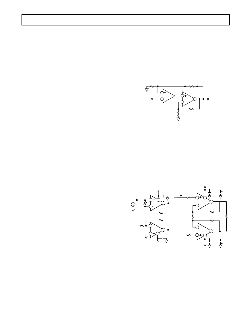
Dual Composite Amplifier
A composite amplifier uses two different op amps together in a
circuit to yield an overall performance that has some of the
advantages of each op amp. In the case of the AD816, two
composite amplifiers can be constructed that offer the low noise
of the receiver amps in addition to the high current output of
the driver amps.
The circuit in Figure 51 shows an example of such a circuit. It
uses receiver amp R1 for the low noise first stage and driver D1
for the high output current second stage. Both local and overall
feedback are used to get the desired response.
6
4
5
V
OUT
2
3
R1
D1
V
IN
Figure 51. AD816 Composite Amplifier
Creating Differential Signals
If only a single-ended signal is available to drive the AD816 and
a differential output signal is desired, a circuit can be used to
perform the single-ended to differential conversion.
The circuit shown in Figure 52 performs this function. It uses
the AD816 with the gain of one receiver set at +1 and the gain
of the other at –1. The 1 k
resistor across the input terminals
of the follower makes the noise gain (NG = 2) equal to the
inverter’s. The two receiver outputs then differentially drive the
inputs to the AD816 driver with no common-mode signal to first
order.
6
4
5
8
+15V
10
7
–15V
R
F
499
R
L
9
11
0.1μF
10μF
R
G
100
R
F
499
0.1μF
10μF
1
8
+15V
0.1μF
2
1k
4
–15V
1k
7
0.1μF
6
5
1k
3
AD816
100
100
1k
AD816
AD816
AD816
RECEIVER #1
RECEIVER #2
DRIVER #1
DRIVER #2
Figure 52. Differential Driver with Single-Ended
Differential Converter
相關(guān)PDF資料 |
PDF描述 |
|---|---|
| AD8170AN | 250 MHz, 10 ns Switching Multiplexers w/Amplifier |
| AD8170AR | 250 MHz, 10 ns Switching Multiplexers w/Amplifier |
| AD8170-EB | 250 MHz, 10 ns Switching Multiplexers w/Amplifier |
| AD8170AR-REEL | 250 MHz, 10 ns Switching Multiplexers w/Amplifier |
| AD8174-EB | 250 MHz, 10 ns Switching Multiplexers w/Amplifier |
相關(guān)代理商/技術(shù)參數(shù) |
參數(shù)描述 |
|---|---|
| AD816AVR | 制造商:Rochester Electronics LLC 功能描述:ADSL TRANSCEIVER - Bulk |
| AD816AY | 制造商:Rochester Electronics LLC 功能描述:ADSL TRANSCEIVER - Bulk |
| AD816AYR | 制造商:未知廠家 制造商全稱:未知廠家 功能描述:Analog IC |
| AD816AYS | 制造商:Rochester Electronics LLC 功能描述:- Bulk |
發(fā)布緊急采購(gòu),3分鐘左右您將得到回復(fù)。