- 您現在的位置:買賣IC網 > PDF目錄373939 > AD8176 (Analog Devices, Inc.) 475 MHz, Triple 16 】 9 Video Crosspoint Switch PDF資料下載
參數資料
| 型號: | AD8176 |
| 廠商: | Analog Devices, Inc. |
| 英文描述: | 475 MHz, Triple 16 】 9 Video Crosspoint Switch |
| 中文描述: | 475兆赫,三16】9視頻交叉點開關 |
| 文件頁數: | 27/32頁 |
| 文件大小: | 489K |
| 代理商: | AD8176 |
第1頁第2頁第3頁第4頁第5頁第6頁第7頁第8頁第9頁第10頁第11頁第12頁第13頁第14頁第15頁第16頁第17頁第18頁第19頁第20頁第21頁第22頁第23頁第24頁第25頁第26頁當前第27頁第28頁第29頁第30頁第31頁第32頁
Preliminary Technical Data
AD8176
this error. This distorts the output signal from the ideal
response compared to the case when the two outputs are
balanced.
Decoupling
The signal path of the AD8176 is based on high open loop gain
amplifiers with negative feedback. Dominant-pole compensation
is used on-chip to stabilize these amplifiers over the range of
expected applied swing and load conditions. To guarantee this
designed stability, proper supply decoupling is necessary with
respect to both the differential control loops and the common-
mode control loops of the signal path. Signal-generated
currents must return to their sources through low impedance
paths at all frequencies in which there is still loop gain (up to
700 MHz at a minimum).
The signal path compensation capacitors in the AD8176 are
connected to the VNEG supply. At high frequencies, this limits
the power supply rejection ratio (PSRR) from the VNEG supply
to a lower value than that from the VPOS supply. If given a
choice, an application board should be designed such that the
VNEG power is supplied from a low inductance plane, subject
to a least amount of noise.
VOCM_CMENCON and VOCM_CMENCOFF are high speed
common-mode control loops of all output drivers. In the single-
ended output sense, there is no rejection from noise on these
inputs to the outputs. For this reason, care must be taken to
produce low noise sources over the entire range of frequencies
of interest. This is not only important to single-ended
operation, but to differential operation, as there is a common-
mode-to-differential gain conversion that becomes greater at
higher frequencies.
VOCM_CMENCON and VOCM_CMENCOFF are internally
buffered to prevent transients flowing into or out of these inputs
from acting on the source impedance and becoming sources of
crosstalk.
Power Dissipation
Calculation of Power Dissipation
Rev. PrA | Page 27 of 32
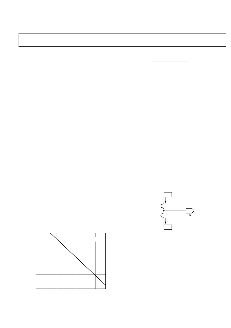
8
415
85
M
AMBIENT TEMPERATURE (°C)
5
6
7
25
35
45
55
65
75
T
J
= 150°C
0
Figure 25. Maximum Die Power Dissipation vs. Ambient Temperature
The curve in Figure 25 was calculated from
JA
AMBIENT
T
MAX
θ
JUNCTION
T
MAX
D
P
=
,
,
(1)
As an example, if the AD8176 is enclosed in an environment at
45
°
C (T
A
), the total on-chip dissipation under all load and
supply conditions must not be allowed to exceed 7.0 W.
When calculating on-chip power dissipation, it is necessary to
include the power dissipated in the output devices due to
current flowing in the loads. For a sinusoidal output about
ground and symmetrical split supplies, the on-chip power
dissipation due the load can be approximated by
(
RMS
UTPUT
O
POS
OUT
D
,
,
)
RMS
OUTPUT
I
V
V
P
,
×
=
(2)
For nonsinusoidal output, the power dissipation should be
calculated by integrating the on-chip voltage drop across the
output devices multiplied by the load current over one period.
The user can subtract the quiescent current for the Class AB
output stage when calculating the loaded power dissipation. For
each output stage driving a load, subtract a quiescent power,
according to
(
)
NEG
POS
Q
OUT
D
V
V
P
,
,
QUIESCENT
OUTPUT
I
,
×
=
(3)
where
I
OUTPUT, QUIESCENT
= 1.65 mA for each single-ended output
pin for the AD8176.
For each disabled RGB output channel, the quiescent
power supply current in VPOS and VNEG drops by approxi-
mately 34 mA.
QNPN
QPNP
V
NEG
V
POS
V
OUTPUT
I
OUTPUT
I
O, QUIESCENT
I
O, QUIESCENT
0
Figure 26. Simplified Output Stage
An example:
For the
AD8176, with an ambient temperature of
85°C, all nine RGB output channels driving 1 V
rms
into 100 Ω
loads, and power supplies at ±2.5 V, follow these steps:
1.
Calculate power dissipation of AD8176 using data sheet
quiescent currents. Neglecting V
DD
current, as it is
insignificant.
(
VPOS
POS
QUIESCENT
D
I
V
P
,
(
mA
600
V
5
,
QUIESCENT
D
P
) (
+
)
VNEG
NEG
(
5
I
V
×
×
=
(4)
)
)
W
3
mA
600
V
=
×
+
×
=
2.
Calculate power dissipation from loads. For a differential
output and ground-referenced load, the output power is
symmetrical in each output phase.
相關PDF資料 |
PDF描述 |
|---|---|
| AD8176ABPZ | 475 MHz, Triple 16 】 9 Video Crosspoint Switch |
| AD8178 | 450 MHz, Triple 16 】 5 Video Crosspoint Switch |
| AD8178ABPZ1 | 450 MHz, Triple 16 】 5 Video Crosspoint Switch |
| AD8178-EVALZ1 | 450 MHz, Triple 16 】 5 Video Crosspoint Switch |
| AD817 | High Speed, Low Power Wide Supply Range Amplifier(高速,低功耗,寬電源范圍放大器) |
相關代理商/技術參數 |
參數描述 |
|---|---|
| AD8176ABPZ | 功能描述:IC VIDEO CROSSPOINT SWIT 676BGA RoHS:是 類別:集成電路 (IC) >> 接口 - 模擬開關,多路復用器,多路分解器 系列:- 其它有關文件:STG4159 View All Specifications 標準包裝:5,000 系列:- 功能:開關 電路:1 x SPDT 導通狀態電阻:300 毫歐 電壓電源:雙電源 電壓 - 電源,單路/雙路(±):±1.65 V ~ 4.8 V 電流 - 電源:50nA 工作溫度:-40°C ~ 85°C 安裝類型:表面貼裝 封裝/外殼:7-WFBGA,FCBGA 供應商設備封裝:7-覆晶 包裝:帶卷 (TR) |
| AD8176-EVAL | 制造商:AD 制造商全稱:Analog Devices 功能描述:475 MHz, Triple 16 】 9 Video Crosspoint Switch |
| AD8177 | 制造商:AD 制造商全稱:Analog Devices 功能描述:500 MHz, Triple 16 】 5 Video Crosspoint Switch |
| AD8177ABPZ | 功能描述:IC VIDEO CROSSPOINT SWIT 676BGA RoHS:是 類別:集成電路 (IC) >> 接口 - 模擬開關,多路復用器,多路分解器 系列:- 其它有關文件:STG4159 View All Specifications 標準包裝:5,000 系列:- 功能:開關 電路:1 x SPDT 導通狀態電阻:300 毫歐 電壓電源:雙電源 電壓 - 電源,單路/雙路(±):±1.65 V ~ 4.8 V 電流 - 電源:50nA 工作溫度:-40°C ~ 85°C 安裝類型:表面貼裝 封裝/外殼:7-WFBGA,FCBGA 供應商設備封裝:7-覆晶 包裝:帶卷 (TR) |
| AD8177-EVALZ | 制造商:AD 制造商全稱:Analog Devices 功能描述:500 MHz, Triple 16 】 5 Video Crosspoint Switch |
發布緊急采購,3分鐘左右您將得到回復。