- 您現在的位置:買賣IC網 > PDF目錄373941 > AD8205YR-REEL7 (ANALOG DEVICES INC) 10 MHz, 20 V/µs, G = 1, 2, 4, 8 iCMOS® Programmable Gain Instrumentation Amplifier; Package: EVALUATION BOARDS; No of Pins: -; Temperature Range: Industrial PDF資料下載
參數資料
| 型號: | AD8205YR-REEL7 |
| 廠商: | ANALOG DEVICES INC |
| 元件分類: | 運動控制電子 |
| 英文描述: | 10 MHz, 20 V/µs, G = 1, 2, 4, 8 iCMOS® Programmable Gain Instrumentation Amplifier; Package: EVALUATION BOARDS; No of Pins: -; Temperature Range: Industrial |
| 中文描述: | OP-AMP, 4500 uV OFFSET-MAX, PDSO8 |
| 封裝: | MS-012AA, SOIC-8 |
| 文件頁數: | 8/12頁 |
| 文件大小: | 308K |
| 代理商: | AD8205YR-REEL7 |
AD8205
THEORY OF OPERATION
The AD8205 is a single-supply difference amplifier that uses a
unique architecture to accurately amplify small differential cur-
rent shunt voltages in the presence of rapidly changing common-
mode voltages. It is offered in both packaged and die form.
Rev. 0 | Page 8 of 12
In typical applications, the AD8205 is used to measure current
by amplifying the voltage across a current shunt placed across
the inputs.
The gain of the AD8205 is 50 V/V, with an accuracy of 1.2%.
This accuracy is guaranteed over the operating temperature
range of 40°C to +125°C. The die temperature range is 40°C
to +150°C with a guaranteed gain accuracy of 1.3%.
The input offset is less than 2 mV referred to the input at 25°C,
and 4.5 mV maximum referred to the input over the full operat-
ing temperature range for the packaged part. The die input off-
set is less than 6 mV referred to the input over the die operating
temperature range.
The AD8205 operates with a single supply from 4.5 V to 10 V (ab-
solute maximum = 12.5 V). The supply current is less than 2 mA.
High accuracy trimming of the internal resistors allows the
AD8205 to have a common-mode rejection ratio better than
78 dB from dc to 20 kHz. The common-mode rejection ratio
over the operating temperature is 76 dB for both the die and
packaged part.
The output offset can be adjusted from 0.05 V to 4.8 V (V+ =
5 V) for unipolar and bipolar operation.
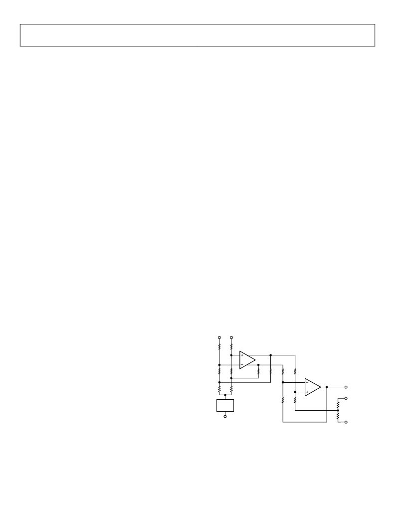
The AD8205 consists of two amplifiers (A1 and A2), a resistor
network, small voltage reference, and a bias circuit (not shown),
see Figure 13.
The set of input attenuators preceding A1 consist of R
A
, R
B
, and
R
C
, which reduce the common-mode voltage to match the input
voltage range of A1. The two attenuators form a balanced bridge
network. When the bridge is balanced, the differential voltage
created by a common-mode voltage is 0 V at the inputs of A1.
The input attenuation ratio is 1/16.7. The combined series resis-
tance of R
A
, R
B
, and R
C
is approximately 200 k ± 20%.
By attenuating the voltages at Pin 1 and Pin 8, the A1 amplifier
inputs are held within the power supply range, even if Pin 1 and
Pin 8 exceed the supply or fall below common (ground). A ref-
erence voltage of 250 mV biases the attenuator above ground.
This allows the amplifier to operate in the presence of negative
common-mode voltages.
The input network also attenuates normal (differential) mode
voltages. A1 amplifies the attenuated signal by 26. The input and
output of this amplifier are differential to maximize the ac
common-mode rejection.
A2 converts the differential voltage from A1 into a single-ended
signal and provides further amplification. The gain of this sec-
ond stage is 32.15.
The reference inputs, V
REF
1 and V
REF
2, are tied through resistors
to the positive input of A2, which allows the output offset to be
adjusted anywhere in the output operating range. The gain is
1 V/V from the reference pins to the output when the reference
pins are used in parallel. The gain is 0.5 V/V when they are used
to divide the supply.
The ratios of Resistors R
A
, R
B
, R
C
, R
D
, and R
F
are trimmed to a
high level of precision to allow the common-mode rejection
ratio to exceed 80 dB. This is accomplished by laser trimming
the resistor ratio matching to better than 0.01%.
The total gain of 50 is made up of the input attenuation of
1/16.7 multiplied by the first stage gain of 26 and the second
stage gain of 32.15.
The output stage is Class A with a PNP pull-up transistor and a
300 μA current sink pull-down.
0
AD8205
+IN
–IN
250mV
GND
A1
A2
R
A
R
A
R
B
R
B
R
F
R
F
R
D
R
D
R
E
R
F
R
C
R
C
V
OUT
R
REF
R
REF
V
REF
1
V
REF
2
Figure 13. Simplified Schematic
相關PDF資料 |
PDF描述 |
|---|---|
| AD8205 | Single-Supply 42 V System Difference Amplifier |
| AD8205YR | +3.3V, 2.5Gbps/2.7Gbps, SDH/SONET 4:1 Serializer with Clock Synthesis |
| AD8206 | Precision, Dual-Channel Difference Amplifier |
| AD8210 | High Voltage, Bidirectional Current Shunt Monitor |
| AD8210_06 | High Voltage, Bidirectional Current Shunt Monitor |
相關代理商/技術參數 |
參數描述 |
|---|---|
| AD8205YRZ | 功能描述:IC AMP DIFF 8SOIC RoHS:是 類別:集成電路 (IC) >> Linear - Amplifiers - Instrumentation 系列:- 產品培訓模塊:Differential Circuit Design Techniques for Communication Applications 標準包裝:1 系列:- 放大器類型:RF/IF 差分 電路數:1 輸出類型:差分 轉換速率:9800 V/µs 增益帶寬積:- -3db帶寬:2.9GHz 電流 - 輸入偏壓:3µA 電壓 - 輸入偏移:- 電流 - 電源:40mA 電流 - 輸出 / 通道:- 電壓 - 電源,單路/雙路(±):3 V ~ 3.6 V 工作溫度:-40°C ~ 85°C 安裝類型:表面貼裝 封裝/外殼:16-VQFN 裸露焊盤,CSP 供應商設備封裝:16-LFCSP-VQ 包裝:剪切帶 (CT) 產品目錄頁面:551 (CN2011-ZH PDF) 其它名稱:ADL5561ACPZ-R7CT |
| AD8205YRZ-R7 | 功能描述:IC AMP DIFF 8SOIC RoHS:是 類別:集成電路 (IC) >> Linear - Amplifiers - Instrumentation 系列:- 標準包裝:1,000 系列:- 放大器類型:電壓反饋 電路數:4 輸出類型:滿擺幅 轉換速率:33 V/µs 增益帶寬積:20MHz -3db帶寬:30MHz 電流 - 輸入偏壓:2nA 電壓 - 輸入偏移:3000µV 電流 - 電源:2.5mA 電流 - 輸出 / 通道:30mA 電壓 - 電源,單路/雙路(±):4.5 V ~ 16.5 V,±2.25 V ~ 8.25 V 工作溫度:-40°C ~ 85°C 安裝類型:表面貼裝 封裝/外殼:14-SOIC(0.154",3.90mm 寬) 供應商設備封裝:14-SOIC 包裝:帶卷 (TR) |
| AD8205YRZ-RL | 功能描述:IC AMP DIFF 8SOIC RoHS:是 類別:集成電路 (IC) >> Linear - Amplifiers - Instrumentation 系列:- 標準包裝:1,000 系列:- 放大器類型:電壓反饋 電路數:4 輸出類型:滿擺幅 轉換速率:33 V/µs 增益帶寬積:20MHz -3db帶寬:30MHz 電流 - 輸入偏壓:2nA 電壓 - 輸入偏移:3000µV 電流 - 電源:2.5mA 電流 - 輸出 / 通道:30mA 電壓 - 電源,單路/雙路(±):4.5 V ~ 16.5 V,±2.25 V ~ 8.25 V 工作溫度:-40°C ~ 85°C 安裝類型:表面貼裝 封裝/外殼:14-SOIC(0.154",3.90mm 寬) 供應商設備封裝:14-SOIC 包裝:帶卷 (TR) |
| AD8206 | 制造商:AD 制造商全稱:Analog Devices 功能描述:Single-Supply, 42 V System Difference Amplifier |
| AD8206_05 | 制造商:AD 制造商全稱:Analog Devices 功能描述:Single-Supply, 42 V System Difference Amplifier |
發布緊急采購,3分鐘左右您將得到回復。