- 您現(xiàn)在的位置:買賣IC網(wǎng) > PDF目錄373942 > AD828 (Analog Devices, Inc.) Dual, Low Power Video Op Amp PDF資料下載
參數(shù)資料
| 型號: | AD828 |
| 廠商: | Analog Devices, Inc. |
| 英文描述: | Dual, Low Power Video Op Amp |
| 中文描述: | 雙通道,低功耗視頻運(yùn)算放大器 |
| 文件頁數(shù): | 10/12頁 |
| 文件大小: | 256K |
| 代理商: | AD828 |
AD828
REV. B
–10–
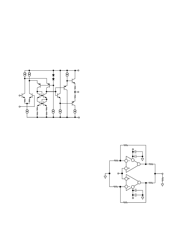
THEORY OF OPERATION
The AD828 is a low cost, dual video operational amplifier
designed to excel in high performance, high output current video
applications.
The AD828 (Figure 40) consists of a degenerated NPN differen-
tial pair driving matched PNPs in a folded-cascode gain stage.
The output buffer stage employs emitter followers in a class AB
amplifier that delivers the necessary current to the load while
maintaining low levels of distortion.
The AD828 will drive terminated cables and capacitive loads of
10 pF or less. As the closed-loop gain is increased, the AD828
will drive heavier cap loads without oscillating.
–
IN
+IN
OUTPUT
+V
S
–
V
S
Figure 40. AD828 Simplified Schematic
INPUT CONSIDERATIONS
An input protection resistor (R
IN
in Figure 34) is required in cir-
cuits where the input to the AD828 will be subjected to transient
or continuous overload voltages exceeding the
±
6 V maximum
differential limit. This resistor provides protection for the input
transistors by limiting their maximum base current.
For high performance circuits, it is recommended that a “bal-
ancing” resistor be used to reduce the offset errors caused by
bias current flowing through the input and feedback resistors.
The balancing resistor equals the parallel combination of R
IN
and R
F
and thus provides a matched impedance at each input
terminal. The offset voltage error will then be reduced by more
than an order of magnitude.
APPLYING THE AD828
The AD828 is a breakthrough dual amp that delivers precision
and speed at low cost with low power consumption. The AD828
offers excellent static and dynamic matching characteristics,
combined with the ability to drive heavy resistive loads.
As with all high frequency circuits, care should be taken to main-
tain overall device performance as well as their matching. The
following items are presented as general design considerations.
Circuit Board Layout
Input and output runs should be laid out so as to physically
isolate them from remaining runs. In addition, the feedback
resistor of each amplifier should be placed away from the feedback
resistor of the other amplifier, since this greatly reduces interamp
coupling.
Choosing Feedback and Gain Resistors
In order to prevent the stray capacitance present at each
amplifier’s summing junction from limiting its performance, the
feedback resistors should be
≤
1 k
. Since the summing junction
capacitance may cause peaking, a small capacitor (1 pF–5 pF)
may be paralleled with Rf to neutralize this effect. Finally, sock-
ets should be avoided, because of their tendency to increase
interlead capacitance.
Power Supply Bypassing
Proper power supply decoupling is critical to preserve the integ-
rity of high frequency signals. In carefully laid out designs,
decoupling capacitors should be placed in close proximity to the
supply pins, while their lead lengths should be kept to a mini-
mum. These measures greatly reduce undesired inductive effects
on the amplifier’s response.
Though two 0.1
μ
F capacitors will typically be effective in de-
coupling the supplies, several capacitors of different values can
be paralleled to cover a wider frequency range.
PARALLEL AMPS PROVIDE 100 mA TO LOAD
By taking advantage of the superior matching characteristics of
the AD828, enhanced performance can easily be achieved by
employing the circuit in Figure 41. Here, two identical cells are
paralleled to obtain even higher load driving capability than that
of a single amplifier (100 mA min guaranteed). R1 and R2 are
included to limit current flow between amplifier outputs that
would arise in the presence of any residual mismatch.
2
+V
S
V
IN
V
OUT
3
8
1k
R2
5
–
V
S
R
L
1/2
AD828
1/2
AD828
1 F
0.1 F
7
5
6
1
1 F
0.1 F
4
R1
5
1k
1k
1k
Figure 41. Parallel Amp Configuration
相關(guān)PDF資料 |
PDF描述 |
|---|---|
| AD828AN | Dual, Low Power Video Op Amp |
| AD828AR | Dual, Low Power Video Op Amp |
| AD8300 | +3 Volt, Serial Input Complete 12-Bit DAC(串行輸入完備的12位D/A轉(zhuǎn)換器) |
| AD8302ARU-REEL | LF.2.7 GHz RF/IF Gain and Phase Detector |
| AD8302 | LF.2.7 GHz RF/IF Gain and Phase Detector |
相關(guān)代理商/技術(shù)參數(shù) |
參數(shù)描述 |
|---|---|
| AD828_02 | 制造商:AD 制造商全稱:Analog Devices 功能描述:Dual, Low Power Video Op Amp |
| AD8280 | 制造商:AD 制造商全稱:Analog Devices 功能描述:Lithium Ion Battery Safety Monitor |
| AD8280-EVALZ | 功能描述:BOARD EVAL FOR AD8280 RoHS:是 類別:編程器,開發(fā)系統(tǒng) >> 評估演示板和套件 系列:- 標(biāo)準(zhǔn)包裝:1 系列:- 主要目的:電信,線路接口單元(LIU) 嵌入式:- 已用 IC / 零件:IDT82V2081 主要屬性:T1/J1/E1 LIU 次要屬性:- 已供物品:板,電源,線纜,CD 其它名稱:82EBV2081 |
| AD8280WASTZ | 功能描述:IC LI-ION BATT MON 48LQFP RoHS:是 類別:集成電路 (IC) >> PMIC - 電池管理 系列:- 標(biāo)準(zhǔn)包裝:2,000 系列:Impedance Track™ 功能:燃料,電量檢測計(jì)/監(jiān)控器 電池化學(xué):鋰離子(Li-Ion) 電源電壓:2.4 V ~ 2.6 V 工作溫度:-40°C ~ 85°C 安裝類型:表面貼裝 封裝/外殼:20-TSSOP(0.173",4.40mm 寬) 供應(yīng)商設(shè)備封裝:20-TSSOP 包裝:帶卷 (TR) 產(chǎn)品目錄頁面:1020 (CN2011-ZH PDF) 配用:BQ27350EVM-ND - BQ27350EVM 其它名稱:296-21665-2 |
| AD8280WASTZ-RL | 功能描述:IC LI-ION BATT MON 48LQFP RoHS:是 類別:集成電路 (IC) >> PMIC - 電池管理 系列:- 產(chǎn)品培訓(xùn)模塊:Lead (SnPb) Finish for COTS Obsolescence Mitigation Program 標(biāo)準(zhǔn)包裝:2,500 系列:- 功能:電池監(jiān)控器 電池化學(xué):堿性,鋰離子,鎳鎘,鎳金屬氫化物 電源電壓:1 V ~ 5.5 V 工作溫度:-40°C ~ 85°C 安裝類型:表面貼裝 封裝/外殼:SOT-23-6 供應(yīng)商設(shè)備封裝:SOT-6 包裝:帶卷 (TR) |
發(fā)布緊急采購,3分鐘左右您將得到回復(fù)。