- 您現在的位置:買賣IC網 > PDF目錄373942 > AD828 (Analog Devices, Inc.) Dual, Low Power Video Op Amp PDF資料下載
參數資料
| 型號: | AD828 |
| 廠商: | Analog Devices, Inc. |
| 英文描述: | Dual, Low Power Video Op Amp |
| 中文描述: | 雙通道,低功耗視頻運算放大器 |
| 文件頁數: | 3/12頁 |
| 文件大小: | 256K |
| 代理商: | AD828 |
Parameter
Conditions
V
S
Min
Typ
Max
Unit
OUTPUT CHARACTERISTICS
Output Voltage Swing
R
LOAD
= 500
R
LOAD
= 150
R
LOAD
= 1 k
R
LOAD
= 500
±
5 V
±
5 V
±
15 V
±
15 V
3.3
3.2
13.3
12.8
+1.5,
+3.5
50
40
30
3.8
3.6
13.7
13.4
±
V
±
V
±
V
±
V
R
LOAD
= 500
0, +5 V
±
15 V
±
5 V
0, +5 V
±
15 V
±
V
mA
mA
mA
mA
Output Current
Short-Circuit Current
Output Resistance
MATCHING CHARACTERISTICS
Dynamic
Crosstalk
Gain Flatness Match
Skew Rate Match
DC
Input Offset Voltage Match
Input Bias Current Match
Open-Loop Gain Match
Common-Mode Rejection Ratio Match V
=
±
12 V, T
MIN
to T
MAX
Power Supply Rejection Ratio Match
POWER SUPPLY
Operating Range
90
8
Open Loop
f = 5 MHz
G = +1, f = 40 MHz
G = –1
±
15 V
±
15 V
±
15 V
–80
0.2
10
dB
dB
V/
μ
s
T
MIN
to T
MAX
T
MIN
to T
MAX
V
O
=
±
10 V, R
= 1 k
, T
MIN
to T
MAX
±
5 V,
±
15 V
±
5 V,
±
15 V
±
15 V
±
15 V
0.5
0.06
0.01
100
100
2
0.8
0.15
mV
μ
A
mV/V
dB
dB
80
80
±
5 V to
±
15 V, T
MIN
to T
MAX
Dual Supply
Single Supply
±
2.5
+5
±
18
+36
15
15
15
V
V
mA
mA
mA
dB
Quiescent Current
±
5 V
±
5 V
±
5 V
14.0
14.0
T
MIN
to T
MAX
T
MIN
to T
MAX
V
S
=
±
5 V to
±
15 V, T
MIN
to T
MAX
Power Supply Rejection Ratio
80
90
NOTES
1
Full power bandwidth = slew rate/2
π
V
PEAK
.
Specifications subject to change without notice.
AD828
REV. B
–3–
ABSOLUTE MAXIMUM RATINGS
1
Supply Voltage . . . . . . . . . . . . . . . . . . . . . . . . . . . . . . . .
±
18 V
Internal Power Dissipation
2
Plastic DIP (N) . . . . . . . . . . . . . . . . . . See Derating Curves
Small Outline (R) . . . . . . . . . . . . . . . . . See Derating Curves
Input Voltage (Common Mode) . . . . . . . . . . . . . . . . . . . .
±
V
S
Differential Input Voltage . . . . . . . . . . . . . . . . . . . . . . . .
±
6 V
Output Short Circuit Duration . . . . . . . . See Derating Curves
Storage Temperature Range (N, R) . . . . . . . –65
°
C to +125
°
C
Operating Temperature Range . . . . . . . . . . . –40
°
C to +85
°
C
Lead Temperature Range (Soldering 10 sec) . . . . . . . .+300
°
C
NOTES
1
Stresses above those listed under Absolute Maximum Ratings may cause perma-
nent damage to the device. This is a stress rating only; functional operation of the
device at these or any other conditions above those indicated in the operational
section of this specification is not implied. Exposure to absolute maximum rating
conditions for extended periods may affect device reliability.
2
Specification is for device in free air:
8-Lead Plastic DIP Package:
θ
JA
= 100
°
C/Watt
8-Lead SOIC Package:
θ
JA
= 155
°
C/Watt
CAUTION
ESD (electrostatic discharge) sensitive device. Electrostatic charges as high as 4000 V readily
accumulate on the human body and test equipment and can discharge without detection.
Although the AD828 features proprietary ESD protection circuitry, permanent damage may
occur on devices subjected to high-energy electrostatic discharges. Therefore, proper ESD
precautions are recommended to avoid performance degradation or loss of functionality.
2.0
0
–
50
90
1.5
0.5
–
30
1.0
50
70
30
10
–
10
AMBIENT TEMPERATURE
–
C
80
–
40
40
60
20
0
–
20
M
–
8-LEAD MINI-DIP PACKAGE
8-LEAD SOIC PACKAGE
T
J
= +150 C
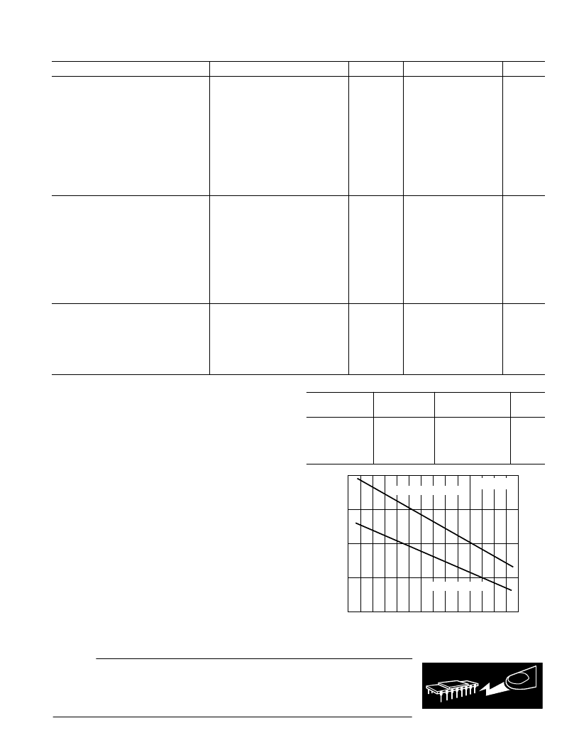
Figure 3. Maximum Power Dissipation vs.
Temperature for Different Package Types
WARNING!
ESD SENSITIVE DEVICE
ORDERING GUIDE
Temperature
Range
Package
Description
Package
Option
Model
AD828AN
AD828AR
AD828AR-REEL7–40
°
C to +85
°
C 7" Tape & Reel
AD828AR-REEL –40
°
C to +85
°
C 13" Tape & Reel
–40
°
C to +85
°
C 8-Lead Plastic DIP
–40
°
C to +85
°
C 8-Lead Plastic SOIC SO-8
N-8
SO-8
SO-8
相關PDF資料 |
PDF描述 |
|---|---|
| AD828AN | Dual, Low Power Video Op Amp |
| AD828AR | Dual, Low Power Video Op Amp |
| AD8300 | +3 Volt, Serial Input Complete 12-Bit DAC(串行輸入完備的12位D/A轉換器) |
| AD8302ARU-REEL | LF.2.7 GHz RF/IF Gain and Phase Detector |
| AD8302 | LF.2.7 GHz RF/IF Gain and Phase Detector |
相關代理商/技術參數 |
參數描述 |
|---|---|
| AD828_02 | 制造商:AD 制造商全稱:Analog Devices 功能描述:Dual, Low Power Video Op Amp |
| AD8280 | 制造商:AD 制造商全稱:Analog Devices 功能描述:Lithium Ion Battery Safety Monitor |
| AD8280-EVALZ | 功能描述:BOARD EVAL FOR AD8280 RoHS:是 類別:編程器,開發系統 >> 評估演示板和套件 系列:- 標準包裝:1 系列:- 主要目的:電信,線路接口單元(LIU) 嵌入式:- 已用 IC / 零件:IDT82V2081 主要屬性:T1/J1/E1 LIU 次要屬性:- 已供物品:板,電源,線纜,CD 其它名稱:82EBV2081 |
| AD8280WASTZ | 功能描述:IC LI-ION BATT MON 48LQFP RoHS:是 類別:集成電路 (IC) >> PMIC - 電池管理 系列:- 標準包裝:2,000 系列:Impedance Track™ 功能:燃料,電量檢測計/監控器 電池化學:鋰離子(Li-Ion) 電源電壓:2.4 V ~ 2.6 V 工作溫度:-40°C ~ 85°C 安裝類型:表面貼裝 封裝/外殼:20-TSSOP(0.173",4.40mm 寬) 供應商設備封裝:20-TSSOP 包裝:帶卷 (TR) 產品目錄頁面:1020 (CN2011-ZH PDF) 配用:BQ27350EVM-ND - BQ27350EVM 其它名稱:296-21665-2 |
| AD8280WASTZ-RL | 功能描述:IC LI-ION BATT MON 48LQFP RoHS:是 類別:集成電路 (IC) >> PMIC - 電池管理 系列:- 產品培訓模塊:Lead (SnPb) Finish for COTS Obsolescence Mitigation Program 標準包裝:2,500 系列:- 功能:電池監控器 電池化學:堿性,鋰離子,鎳鎘,鎳金屬氫化物 電源電壓:1 V ~ 5.5 V 工作溫度:-40°C ~ 85°C 安裝類型:表面貼裝 封裝/外殼:SOT-23-6 供應商設備封裝:SOT-6 包裝:帶卷 (TR) |
發布緊急采購,3分鐘左右您將得到回復。