- 您現在的位置:買賣IC網 > PDF目錄373942 > AD8305 (Analog Devices, Inc.) 100 dB Range (10 nA to 1 mA) Logarithmic Converter PDF資料下載
參數資料
| 型號: | AD8305 |
| 廠商: | Analog Devices, Inc. |
| 英文描述: | 100 dB Range (10 nA to 1 mA) Logarithmic Converter |
| 中文描述: | 100分貝范圍(10 nA的1毫安)對數轉換器 |
| 文件頁數: | 12/20頁 |
| 文件大小: | 1301K |
| 代理商: | AD8305 |
REV. A
–12–
AD8305
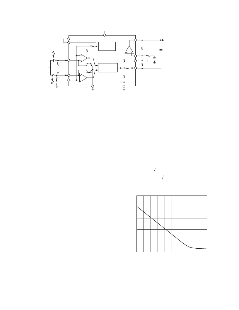
LOG-RATIO APPLICATIONS
It is often desirable to determine the ratio of two currents, for
example, in absorbance measurements. These are commonly used
to assess the attenuation of a passive optical component, such as
an optical filter or variable optical attenuator. In these situations,
a reference detector is used to measure the incident power enter-
ing the component. The exiting power is then measured using a
second detector and the ratio is calculated to determine the
attenuation factor. Since the AD8305 is fundamentally a ratiometric
device, having nearly identical logging systems for both numerator
and denominator (I
PD
and I
REF
, respectively), it can greatly
simplify such measurements.
Figure 5 illustrates the AD8305’s log-ratio capabilities in optical
absorbance measurements. Here a reference detector diode is used
to provide the reference current, I
REF
, proportional to the optical
reference power level. A second detector measures the transmitted
signal power, proportional to I
PD
. The AD8305 calculates the
logarithm of the ratio of these two currents, as shown in
Equation 11, and which is reformulated in power terms in
Equation 12. Both of these equations include the internal factor
of 10,000 introduced by the output offset applied to V
LOG
via pin
VRDZ. If the true (nonoffset) log ratio shown in Equation 4 is
preferred, VRDZ should be grounded to remove the offset. As
already noted, the use of a negative supply at Pin VNEG will
allow both V
LOG
and the buffer output to swing below ground,
and also allow the input pins INPT and IREF to be set to
ground potential. Thus, the AD8305 may also be used to deter-
mine the log ratio of two voltages.
Figure 5 also illustrates how a second order Sallen-Key low-pass
filter can be realized using two external capacitors and one
resistor. Here, the corner frequency is set to 1 kHz and the filter
Q is chosen to provide an optimally flat (overshoot-free) pulse
response. To scale this frequency either up or down, simply
scale the capacitors by the appropriate factor. Note that one of
the resistors needed to realize this filter is the output resistance
of 4.55 k
W
present at Pin VLOG. While this will not ratio
exactly to the external resistor, which may slightly alter the Q of
the filter, the effect on pulse response will be negligible for most
purposes. Note that the gain of the buffer ( 2.5) is an integral
part of this illustrative filter design; in general, the filter may be
redesigned for other closed-loop gains.
The transfer characteristics can be expressed in terms of optical
power. If we assume that the two detectors have equal responsivities,
the relationship is
V
V
P
OUT
SIG
=
0 5
10
10
.
log
Using the identity log
10
(AB) = log
10
A + log
10
B and defining the
attenuation as –10 log
10
(
P
SIG
/
P
REF
), the overall transfer char-
acteristic can be written as
¥
2
50
–
a
P
/
REF
¥
(
)
4
(11)
V
mV dB
OUT
=
(12)
where
a =
Figure 6 illustrates the linear-in-dB relationship between the
absorbance and the output of the circuit in Figure 5.
¥
–
log (
)
10
P
P
SIG
REF
ATTENUATION – dB
2.5
0
50
5
V
L
10
15
20
25
30
35
40
45
2.0
1.5
1.0
0.5
0
Figure 6. Example of an Absorbance Transfer Function
BIAS
GENERATOR
VLOG
COMM
VNEG
VSUM
IREF
0.5V
80k
0.5V
TEMPERATURE
COMPENSATION
V
BE1
6.69k
Q1
COMM
20k
451
VREF
VRDZ
14.2k
Q2
INPT
COMM
2.5 V
VPOS
BFIN
SCAL
VOUT
I
LOG
+5V
+5V
0.5 log
10
PD
I
( )
+ 2
I
PD
I
REF
1k
1nF
1k
1nF
28.0k
44.2k
18nF
REFERENCE
DETECTOR
SIGNAL
DETECTOR
P
REF
P
SIG
33nF
12.1k
–
+
V
BE2
Figure 5. Optical Absorbance Measurement
相關PDF資料 |
PDF描述 |
|---|---|
| AD8305ACP | 100 dB Range (10 nA to 1 mA) Logarithmic Converter |
| AD8305ACP-REEL7 | 100 dB Range (10 nA to 1 mA) Logarithmic Converter |
| AD8306 | 5 MHz-400 MHz 100 dB High Precision Limiting-Logarithmic Amplifier |
| AD8306-EVAL | 5 MHz-400 MHz 100 dB High Precision Limiting-Logarithmic Amplifier |
| AD8306ACHIPS | 5 MHz-400 MHz 100 dB High Precision Limiting-Logarithmic Amplifier |
相關代理商/技術參數 |
參數描述 |
|---|---|
| AD8305_CSURF | 制造商:Analog Devices 功能描述: |
| AD8305ACP | 制造商:AD 制造商全稱:Analog Devices 功能描述:100 dB Range (10 nA to 1 mA) Logarithmic Converter |
| AD8305ACP-R2 | 功能描述:IC LOGARITHM CONV 100DB 16-LFCSP RoHS:否 類別:集成電路 (IC) >> 線性 - 放大器 - 專用 系列:- 產品培訓模塊:Lead (SnPb) Finish for COTS Obsolescence Mitigation Program 標準包裝:60 系列:- 類型:可變增益放大器 應用:CATV 安裝類型:表面貼裝 封裝/外殼:20-WQFN 裸露焊盤 供應商設備封裝:20-TQFN-EP(5x5) 包裝:托盤 |
| AD8305ACP-REEL7 | 制造商:Analog Devices 功能描述:SP Amp LOG Amp Single R-R O/P ±6V/12V 16-Pin LFCSP EP T/R |
| AD8305ACPZ | 制造商:AD 制造商全稱:Analog Devices 功能描述:100 dB Range (10 nA to 1 mA) ogarithmic Converter |
發布緊急采購,3分鐘左右您將得到回復。