- 您現(xiàn)在的位置:買賣IC網(wǎng) > PDF目錄373942 > AD8305 (Analog Devices, Inc.) 100 dB Range (10 nA to 1 mA) Logarithmic Converter PDF資料下載
參數(shù)資料
| 型號: | AD8305 |
| 廠商: | Analog Devices, Inc. |
| 英文描述: | 100 dB Range (10 nA to 1 mA) Logarithmic Converter |
| 中文描述: | 100分貝范圍(10 nA的1毫安)對數(shù)轉換器 |
| 文件頁數(shù): | 14/20頁 |
| 文件大小: | 1301K |
| 代理商: | AD8305 |
REV. A
–14–
AD8305
provisions to offset V
LOG
at the buffer input, allowing measure-
ments over the full range of I
PD
using a single supply. The network
analyzer input impedances were set to 1 M
W
.
AD8305
12
11
10
9
5 6 7 8
COMM COMM COMM COMM
16
15 14 13
1
2
3
4
VSUM VNEG VNEG VPOS
VRDZ
VREF
IREF
INPT
VOUT
SCAL
BFIN
VLOG
0.1 F
OUTPUT
AD8138
EVALUATION
BOARD
A
B
+IN
INPUT R
INPUT A
INPUT B
HP 3577A
NETWORK ANALYZER
+V
S
POWER
SPLITTER
1nF
1k
R1
1k
1nF
R2
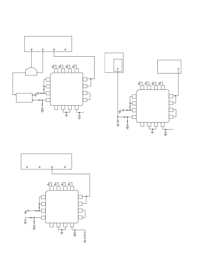
Figure 11. Configuration for Logarithmic
Amplifier Bandwidth Measurement
The setup shown in Figure 11 was used for frequency response
measurements of the logarithmic amplifier section. The AD8138
output is offset to 1.5 V dc and modulated to a depth of 5% at
frequency. R1 is chosen (over a wide range of values up to
1.0 G
W
) to provide I
PD
. The buffer was used to deload VLOG
from the measurement system.
AD8305
12
11
10
9
5 6 7 8
COMM COMM COMM COMM
16
15 14 13
1
2
3
4
VSUM VNEG VNEG VPOS
VRDZ
VREF
IREF
INPT
VOUT
SCAL
BFIN
VLOG
0.1 F
SOURCE
TRIGGER
CHANNEL 1 CHANNEL 2
HP 89410A
1nF
1k
1k
1nF
R1
200k
ALKALINE
“D” CELL
ALKALINE
“D” CELL
+
+
+
+
Figure 12. Configuration for Noise Spectral
Density Measurement
The configuration in Figure 12 is used to measure the noise
performance. Batteries provide both the supply voltage and the
input current in order to minimize the introduction of spurious
noise and ground loop effects. The entire evaluation system,
including the current setting resistors, is mounted in a closed
aluminum enclosure to provide additional shielding to external
noise sources.
AD8305
12
11
10
9
5 6 7 8
COMM COMM COMM COMM
16
15 14 13
1
2
3
4
VSUM VNEG VNEG VPOS
VRDZ
VREF
IREF
INPT
VOUT
SCAL
BFIN
VLOG
0.1 F
1nF1k
R1
1k
1nF
200k
CH A
9213
LECROY 9210
CH1
TDS5104
+V
S
Figure 13. Configuration for Logarithmic
Amplifier Pulse Response Measurement
Figure 13 shows the setup used to make the pulse response
measurements. As with the bandwidth measurement, the VLOG
is connected directly to BFIN and the buffer amplifier is config-
ured for unity gain. The buffer’s output is connected through a
short cable to the TDS5104 scope with input impedance set to
1 M
W
. The LeCroy’s output is offset to create the initial pedestal
current for a given value of R1, the pulse then creates one-decade
current step.
EVALUATION BOARD
An evaluation board is available for the AD8305, the schematic
for which is shown in Figure 16. It can be configured for a wide
variety of experiments. The buffer gain is factory-set to unity,
providing a slope of 200 mV/decade, and the intercept is set to 1 nA.
Table I describes the various configuration options.
相關PDF資料 |
PDF描述 |
|---|---|
| AD8305ACP | 100 dB Range (10 nA to 1 mA) Logarithmic Converter |
| AD8305ACP-REEL7 | 100 dB Range (10 nA to 1 mA) Logarithmic Converter |
| AD8306 | 5 MHz-400 MHz 100 dB High Precision Limiting-Logarithmic Amplifier |
| AD8306-EVAL | 5 MHz-400 MHz 100 dB High Precision Limiting-Logarithmic Amplifier |
| AD8306ACHIPS | 5 MHz-400 MHz 100 dB High Precision Limiting-Logarithmic Amplifier |
相關代理商/技術參數(shù) |
參數(shù)描述 |
|---|---|
| AD8305_CSURF | 制造商:Analog Devices 功能描述: |
| AD8305ACP | 制造商:AD 制造商全稱:Analog Devices 功能描述:100 dB Range (10 nA to 1 mA) Logarithmic Converter |
| AD8305ACP-R2 | 功能描述:IC LOGARITHM CONV 100DB 16-LFCSP RoHS:否 類別:集成電路 (IC) >> 線性 - 放大器 - 專用 系列:- 產(chǎn)品培訓模塊:Lead (SnPb) Finish for COTS Obsolescence Mitigation Program 標準包裝:60 系列:- 類型:可變增益放大器 應用:CATV 安裝類型:表面貼裝 封裝/外殼:20-WQFN 裸露焊盤 供應商設備封裝:20-TQFN-EP(5x5) 包裝:托盤 |
| AD8305ACP-REEL7 | 制造商:Analog Devices 功能描述:SP Amp LOG Amp Single R-R O/P ±6V/12V 16-Pin LFCSP EP T/R |
| AD8305ACPZ | 制造商:AD 制造商全稱:Analog Devices 功能描述:100 dB Range (10 nA to 1 mA) ogarithmic Converter |
發(fā)布緊急采購,3分鐘左右您將得到回復。