- 您現在的位置:買賣IC網 > PDF目錄373942 > AD8305ACP (ANALOG DEVICES INC) 100 dB Range (10 nA to 1 mA) Logarithmic Converter PDF資料下載
參數資料
| 型號: | AD8305ACP |
| 廠商: | ANALOG DEVICES INC |
| 元件分類: | 運動控制電子 |
| 英文描述: | 100 dB Range (10 nA to 1 mA) Logarithmic Converter |
| 中文描述: | LOG OR ANTILOG AMPLIFIER, QCC16 |
| 封裝: | 3 X 3 MM, MINIATURE, MO-220-VEED-2, LFCSP-16 |
| 文件頁數: | 11/20頁 |
| 文件大小: | 1301K |
| 代理商: | AD8305ACP |
REV. A
AD8305
–11–
The dynamic response of this overall input system is influenced by
the external RC networks connected from the two inputs (INPT,
IREF) to ground. These are required to stabilize the input systems
over the full current range. The bandwidth changes with the
input current due to the widely varying pole frequency. The RC
network adds a zero to the input system to ensure stability over the
full range of input current levels. The network values shown in
Figure 2 will usually suffice, but some experimentation may be
necessary when the photodiode capacitance is high.
Although the two current inputs are similar, some care is needed
to operate the reference input at extremes of current (<100 nA)
and temperature (<0
∞
C). Modifying the RC network to 4.7 nF
and 2 k
W
will allow operation to –40
∞
C at 10 nA. By inspecting
the transient response to perturbations in I
REF
at representative
current levels, the capacitor value can be adjusted to provide fast
rise and fall times with acceptable settling. To fine tune the net-
work zero, the resistor value should be adjusted.
CALIBRATION
The AD8305 has a nominal slope and intercept of 200 mV/decade
and 1 nA, respectively. These values are untrimmed and the
slope alone may vary as much as 7.5% over temperature. For
this reason, it is recommended that a simple calibration be done
to achieve increased accuracy.
I
PD
– A
1.4
0
1n
V
L
–
1.2
1.0
0.8
0.6
0.4
0.2
4
3
2
1
0
–1
–2
–3
IDEAL OUTPUT
CALIBRATED ERROR
MEASURED OUTPUT
UNCALIBRATED ERROR
E
10n
100n
1
10
100
1m
10m
Figure 3. Using Two-Point Calibration to Increase
Measurement Accuracy
Figure 3 shows the improvement in accuracy when using a two-
point calibration method. To perform this calibration, apply two
known currents,
I
1
and
I
2
, in the linear operating range between
10 nA and 1 mA. Measure the resulting output,
V
1
and
V
2
,
respectively, and calculate the slope
m
and intercept
b
.
m
V
V
I
I
=
(
)
( )
( )
]
1
2
10
1
10
2
–
/ log
– log
(7)
b V
m
I
¥
( )
1
10
1
–
log
(8)
The same calibration could be performed with two known opti-
cal powers,
P
1
and
P
2
. This allows for calibration of the entire
measurement system while providing a simplified relationship
between the incident optical power and V
LOG
voltage.
m
V
V
P
P
=
(
) (
)
1
2
1
2
–
/
–
(9)
b V
m
P
¥
1
1
–
(10)
The Uncalibrated Error line in Figure 3 was generated assuming
that the slope of the measured output was 200 mV/decade when
in fact it was actually 194 mV/decade. Correcting for this dis-
crepancy decreased measurement error up to 3 dB.
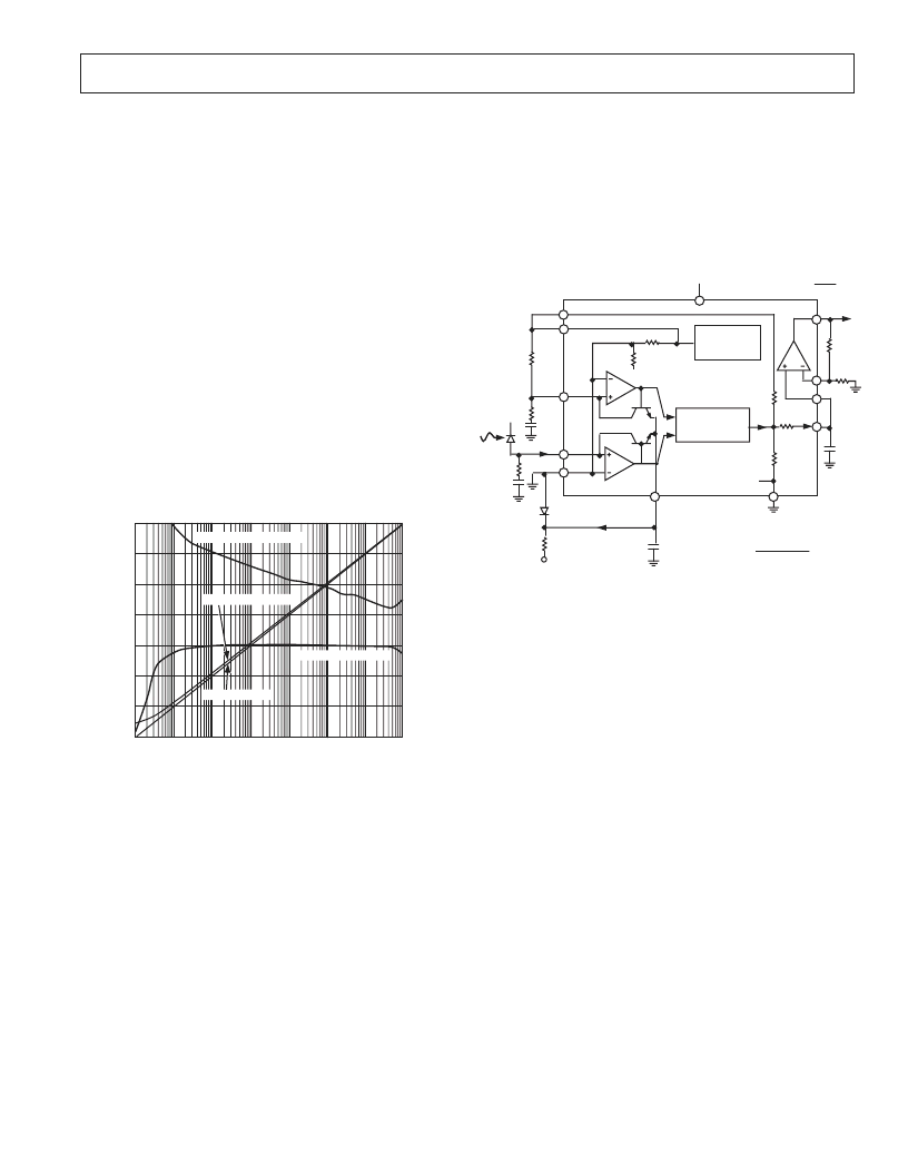
USING A NEGATIVE SUPPLY
Most applications of the AD8305 require only a single supply of
3.0 V to 5.5 V. However, to provide further versatility, dual
supplies may be employed, as illustrated in Figure 4.
BIAS
GENERATOR
VLOG
COMM
VNEG
VSUM
IREF
0.5V
80k
0.5V
TEMPERATURE
COMPENSATION
V
BE1
V
BE2
6.69k
Q1
COMM
20k
451
VREF
VRDZ
14.2k
Q2
INPT
COMM
2.5V
VPOS
BFIN
SCAL
VOUT
I
LOG
I
PD
RREF
200k
0.5 log
10
PD
1nA
( )
1nF
1k
V
BIAS
1nF
1k
12k
5V
C
10nF
8k
–
+
+
V
F
–
C1
V
N
R
S
£
V
N
– V
F
I
q
+ I
SIGMAX
I
SIG
= I
PD
+ I
REF
I
q
+ I
SIG
V
NEG
£
–0.5V
R
S
Figure 4. Negative Supply Application
The use of a negative supply, V
N
, allows the summing node to
be placed at ground level whenever the input transistor (Q1 in
Figure 1) has a sufficiently negative bias on its emitter. When
V
NEG
= –0.5 V, the V
CE
of Q1 and Q2 will be the same as for
the default case when VSUM is grounded. This bias need not
be accurate, and a poorly defined source can be used. The
source does however need to be able to support the quiescent
current as well as the INPT and IREF signal current. For example,
it may be convenient to utilize a forward-biased junction voltage
of about 0.7 V or a Schottky barrier voltage of a little over 0.5 V.
The effect of supply on the dynamic range and accuracy can be
seen in TPC 8.
With the summing node at ground, the AD8305 may now be
used as a voltage-input log amp at either the numerator input,
INPT, or the denominator input, IREF, by inserting a suitably
scaled resistor from the voltage source to the relevant pin. The
overall accuracy for small input voltages is limited by the voltage
offset at the inputs of the JFET op amps.
The use of a negative supply also allows the output to swing
below ground, thereby allowing the intercept to correspond to a
midrange value of I
PD
. However, the voltage V
LOG
remains
referenced to the ACOM pin, and while it does not swing nega-
tive for default operating conditions, it is free to do so. Thus,
adding a resistor from VLOG to the negative supply lowers
all values of VLOG, which raises the intercept. The disadvan-
tage of this method is that the slope is reduced by the shunting
of the external resistor, and the poorly defined ratio of on-
chip and off-chip resistances causes errors in both the slope
and the intercept.
相關PDF資料 |
PDF描述 |
|---|---|
| AD8305ACP-REEL7 | 100 dB Range (10 nA to 1 mA) Logarithmic Converter |
| AD8306 | 5 MHz-400 MHz 100 dB High Precision Limiting-Logarithmic Amplifier |
| AD8306-EVAL | 5 MHz-400 MHz 100 dB High Precision Limiting-Logarithmic Amplifier |
| AD8306ACHIPS | 5 MHz-400 MHz 100 dB High Precision Limiting-Logarithmic Amplifier |
| AD8306AR | 5 MHz-400 MHz 100 dB High Precision Limiting-Logarithmic Amplifier |
相關代理商/技術參數 |
參數描述 |
|---|---|
| AD8305ACP-R2 | 功能描述:IC LOGARITHM CONV 100DB 16-LFCSP RoHS:否 類別:集成電路 (IC) >> 線性 - 放大器 - 專用 系列:- 產品培訓模塊:Lead (SnPb) Finish for COTS Obsolescence Mitigation Program 標準包裝:60 系列:- 類型:可變增益放大器 應用:CATV 安裝類型:表面貼裝 封裝/外殼:20-WQFN 裸露焊盤 供應商設備封裝:20-TQFN-EP(5x5) 包裝:托盤 |
| AD8305ACP-REEL7 | 制造商:Analog Devices 功能描述:SP Amp LOG Amp Single R-R O/P ±6V/12V 16-Pin LFCSP EP T/R |
| AD8305ACPZ | 制造商:AD 制造商全稱:Analog Devices 功能描述:100 dB Range (10 nA to 1 mA) ogarithmic Converter |
| AD8305ACPZ-R2 | 功能描述:IC AMP LOG CONV 100DB 16-LFCSP RoHS:是 類別:集成電路 (IC) >> 線性 - 放大器 - 專用 系列:- 產品培訓模塊:Lead (SnPb) Finish for COTS Obsolescence Mitigation Program 標準包裝:60 系列:- 類型:可變增益放大器 應用:CATV 安裝類型:表面貼裝 封裝/外殼:20-WQFN 裸露焊盤 供應商設備封裝:20-TQFN-EP(5x5) 包裝:托盤 |
| AD8305ACPZ-RL7 | 功能描述:IC LOGARITH CONV 100DB 16-LFCSP RoHS:是 類別:集成電路 (IC) >> 線性 - 放大器 - 專用 系列:- 產品培訓模塊:Lead (SnPb) Finish for COTS Obsolescence Mitigation Program 標準包裝:60 系列:- 類型:可變增益放大器 應用:CATV 安裝類型:表面貼裝 封裝/外殼:20-WQFN 裸露焊盤 供應商設備封裝:20-TQFN-EP(5x5) 包裝:托盤 |
發布緊急采購,3分鐘左右您將得到回復。