- 您現在的位置:買賣IC網 > PDF目錄373942 > AD8305ACP (ANALOG DEVICES INC) 100 dB Range (10 nA to 1 mA) Logarithmic Converter PDF資料下載
參數資料
| 型號: | AD8305ACP |
| 廠商: | ANALOG DEVICES INC |
| 元件分類: | 運動控制電子 |
| 英文描述: | 100 dB Range (10 nA to 1 mA) Logarithmic Converter |
| 中文描述: | LOG OR ANTILOG AMPLIFIER, QCC16 |
| 封裝: | 3 X 3 MM, MINIATURE, MO-220-VEED-2, LFCSP-16 |
| 文件頁數: | 13/20頁 |
| 文件大小: | 1301K |
| 代理商: | AD8305ACP |
REV. A
AD8305
–13–
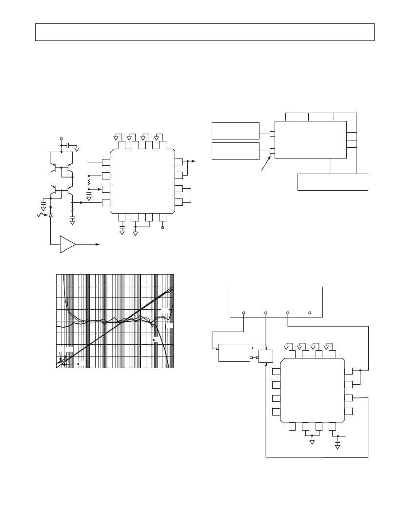
REVERSING THE INPUT POLARITY
Some applications may require interfacing to a circuit that
sources current rather than sinks current, such as connecting to
the cathode side of a photodiode. Figure 7 shows the use of a
current mirror circuit. This allows for simultaneous monitoring
of the optical power at the cathode, and a data recovery path
using a transimpedance amplifier at the anode. The modified
Wilson mirror provides a current gain very close to unity and a
high output resistance. Figure 8 shows measured transfer function
and law conformance performance of the AD8305 in conjunc-
tion with this current mirror interface.
AD8305
12
11
10
9
5 6 7 8
COMM COMM COMM COMM
16
15 14 13
1
2
3
4
VSUM VNEG VNEG VPOS
VRDZ
VREF
IREF
INPT
VOUT
SCAL
BFIN
VLOG
2.5V
0.1 F
5V
0V
0V
1nF
200k
MAT03
MAT03
DATA PATH
5V
0.1 F
TIA
I
I
10nA TO 1mA
I
PD
1k
1nF
OUTPUT
V
OUT
= 0.2
log
10
(I
PD
/1nA)
Figure 7. Wilson Current Mirror for Cathode Interfacing
I
PD
– A
1.4
0
1n
V
L
–
1.2
1.0
0.8
0.6
0.4
0.2
1.00
0.75
0
1.6
0.50
–1.00
–0.75
–0.50
–0.25
0.25
+5V
+3V
5V
5V
+5V
+3V
E
10n
100n
1
10
100
1m
10m
Figure 8. Log Output and Error Using Current
Mirror with Various Supplies
CHARACTERIZATION METHODS
During the characterization of the AD8305, the device was
treated as a precision current-input logarithmic converter, since
it is not practical for several reasons to generate accurate photo-
currents by illuminating a photodiode. The test currents were
generated either by using well calibrated current sources, such
as the Keithley 236, or by using a high value resistor from a
voltage source to the input pin. Great care is needed when using
very small input currents. For example, the triax output connec-
tion from the current generator was used with the guard tied to
VSUM. The input trace on the PC board was guarded by con-
necting adjacent traces to VSUM.
These measures are needed to minimize the risk of leakage
current paths. With 0.5 V as the nominal bias on the INPT pin,
a leakage-path resistance of 1 G
W
to ground would subtract
0.5 nA from the input, which amounts to an error of –0.44 dB for
a source current of 10 nA. Additionally, the very high output
resistance at the input pins and the long cables commonly needed
during characterization allow 60 Hz and RF emissions to introduce
substantial measurement errors. Careful guarding techniques
are essential to reduce the pickup of these spurious signals.
VSUM
VNEG
VPOS
VREF
IREF
INPT
VOUT
BFIN
VLOG
TRIAX CONNECTORS
(SIGNAL – INPT AND IREF
GUARD – VSUM
SHIELD – GROUND)
Figure 9. Primary Characterization Setup
The primary characterization setup shown in Figure 9 is used to
measure V
REF
, the static (dc) performance, logarithmic conform-
ance, slope and intercept, the voltages appearing at pins VSUM,
INPT and IREF, and the buffer offset and V
REF
drift with temper-
ature. To ensure stable operation over the full current range of
I
REF
and temperature extremes, filter components of C1 = 4.7 nF
and R13 = 2 k
W
are used at pin to IREF ground. In some cases,
a fixed resistor between pins VREF and IREF was used in place
of a precision current source. For the dynamic tests, including
noise and bandwidth measurements, more specialized setups
are required.
AD8305
CHARACTERIZATION
BOARD
KEITHLEY 236
KEITHLEY 236
DC MATRIX/DC SUPPLIES/DMM
AD8305
12
11
10
9
5 6 7 8
COMM COMM COMM COMM
16
15 14 13
1
2
3
4
VSUM VNEG VNEG VPOS
VRDZ
VREF
IREF
INPT
VOUT
SCAL
BFIN
VLOG
0.1 F
OUTPUT
AD8138
EVALUATION
BOARD
A
B
+IN
BNC-T
INPUT R
INPUT A
INPUT B
HP 3577A
NETWORK ANALYZER
+V
S
AD8138
PROVIDES DC OFFSET
Figure 10. Configuration for Buffer Amplifier
Bandwidth Measurement
Figure 10 shows the configuration used to measure the buffer
amplifier bandwidth. The AD8138 evaluation board includes
相關PDF資料 |
PDF描述 |
|---|---|
| AD8305ACP-REEL7 | 100 dB Range (10 nA to 1 mA) Logarithmic Converter |
| AD8306 | 5 MHz-400 MHz 100 dB High Precision Limiting-Logarithmic Amplifier |
| AD8306-EVAL | 5 MHz-400 MHz 100 dB High Precision Limiting-Logarithmic Amplifier |
| AD8306ACHIPS | 5 MHz-400 MHz 100 dB High Precision Limiting-Logarithmic Amplifier |
| AD8306AR | 5 MHz-400 MHz 100 dB High Precision Limiting-Logarithmic Amplifier |
相關代理商/技術參數 |
參數描述 |
|---|---|
| AD8305ACP-R2 | 功能描述:IC LOGARITHM CONV 100DB 16-LFCSP RoHS:否 類別:集成電路 (IC) >> 線性 - 放大器 - 專用 系列:- 產品培訓模塊:Lead (SnPb) Finish for COTS Obsolescence Mitigation Program 標準包裝:60 系列:- 類型:可變增益放大器 應用:CATV 安裝類型:表面貼裝 封裝/外殼:20-WQFN 裸露焊盤 供應商設備封裝:20-TQFN-EP(5x5) 包裝:托盤 |
| AD8305ACP-REEL7 | 制造商:Analog Devices 功能描述:SP Amp LOG Amp Single R-R O/P ±6V/12V 16-Pin LFCSP EP T/R |
| AD8305ACPZ | 制造商:AD 制造商全稱:Analog Devices 功能描述:100 dB Range (10 nA to 1 mA) ogarithmic Converter |
| AD8305ACPZ-R2 | 功能描述:IC AMP LOG CONV 100DB 16-LFCSP RoHS:是 類別:集成電路 (IC) >> 線性 - 放大器 - 專用 系列:- 產品培訓模塊:Lead (SnPb) Finish for COTS Obsolescence Mitigation Program 標準包裝:60 系列:- 類型:可變增益放大器 應用:CATV 安裝類型:表面貼裝 封裝/外殼:20-WQFN 裸露焊盤 供應商設備封裝:20-TQFN-EP(5x5) 包裝:托盤 |
| AD8305ACPZ-RL7 | 功能描述:IC LOGARITH CONV 100DB 16-LFCSP RoHS:是 類別:集成電路 (IC) >> 線性 - 放大器 - 專用 系列:- 產品培訓模塊:Lead (SnPb) Finish for COTS Obsolescence Mitigation Program 標準包裝:60 系列:- 類型:可變增益放大器 應用:CATV 安裝類型:表面貼裝 封裝/外殼:20-WQFN 裸露焊盤 供應商設備封裝:20-TQFN-EP(5x5) 包裝:托盤 |
發布緊急采購,3分鐘左右您將得到回復。