- 您現在的位置:買賣IC網 > PDF目錄373942 > AD8306ACHIPS (ANALOG DEVICES INC) 5 MHz-400 MHz 100 dB High Precision Limiting-Logarithmic Amplifier PDF資料下載
參數資料
| 型號: | AD8306ACHIPS |
| 廠商: | ANALOG DEVICES INC |
| 元件分類: | 運動控制電子 |
| 英文描述: | 5 MHz-400 MHz 100 dB High Precision Limiting-Logarithmic Amplifier |
| 中文描述: | LOG OR ANTILOG AMPLIFIER, 395 MHz BAND WIDTH, UUC16 |
| 封裝: | DIE |
| 文件頁數: | 13/16頁 |
| 文件大小: | 397K |
| 代理商: | AD8306ACHIPS |
REV. A
AD8306
–13–
10 mV/dB The AD8031 rail-to-rail op amp, used in both ex-
amples, can swing from 50 mV to 4.95 mV on a single +5 V
supply. If high output current is required (> 10 mA), the AD8051,
which also has rail-to-rail capability but can deliver up to 45 mA
of output current, can be used.
APPLICATIONS
The AD8306 is a versatile and easily applied log-limiting ampli-
fier. Being complete, it can be used with very few external com-
ponents, and most applications can be accommodated using the
simple connections shown in the preceding section. A few ex-
amples of more specialized applications are provided here.
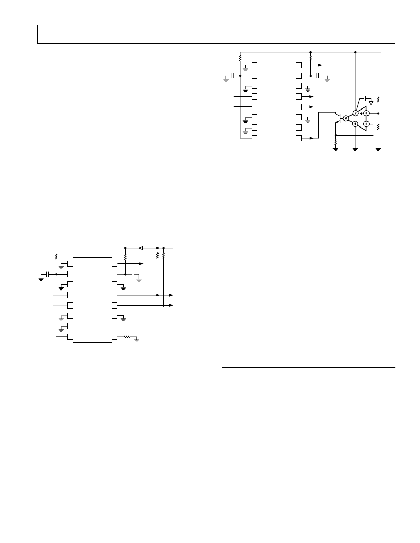
High Output Limiter Loading
The AD8306 can generate a fairly large output power at its
differential limiter output interface. This may be coupled into a
50
grounded load using the narrow-band coupling network
following similar lines to those provided for input matching.
Alternatively, a flux-linked transformer, having a center-tapped
primary, may be used. Even higher output powers can be ob-
tained using emitter-followers. In Figure 31, the supply voltage
to the AD8306 is dropped from 5 V to about 4.2 V, by the
diode. This increases the available swing at each output to about
2 V. Taking both outputs differentially, a square wave output of
4 V p-p can be generated.
1
2
3
4
5
6
7
8
VLOG
VPS2
PADL
LMHI
LMLO
PADL
FLTR
LMDR
COM2
VPS1
PADL
INHI
INLO
PADL
COM1
ENBL
AD8306
9
10
11
14
15
16
0.1
m
F
10
V
R
LIM
RSSI
3V TO 5V
0.1
m
F
10
V
12
13
+5V
IN914
APPROX. 4.2V
R
LOAD
SET R
L
= 5*R
LIM
5V TO 3V
DIFFERENTIAL
OUTPUT = 4V pk-pk
R
LOAD
Figure 31. Increasing Limiter Output Voltage
When operating at high output power levels and high frequen-
cies, very careful attention must be paid to the issue of stability.
Oscillation is likely to be observed when the input signal level is
low, due to the extremely high gain-bandwidth product of the
AD8306 under such conditions. These oscillations will be less
evident when signal-balancing networks are used, operating at
frequencies below 200 MHz, and they will generally be fully
quenched by the signal at input levels of a few dB above the
noise floor.
Modulated Limiter Output
The limiter output stage of the AD8306 also provides an analog
multiplication capability: the amplitude of the output square
wave can be controlled by the current withdrawn from LMDR
(Pin 9). An analog control input of 0 V to +1 V is used to gener-
ate an exactly-proportional current of 0 mA to 10 mA in the npn
transistor, whose collector is held at a fixed voltage of
~
400 mV
by the internal bias in the AD8306. When the input signal is
above the limiting threshold, the output will then be a square-
wave whose amplitude is proportional to the control bias.
1
2
3
4
5
6
7
8
VLOG
VPS2
PADL
LMHI
LMLO
PADL
FLTR
LMDR
COM2
VPS1
PADL
INHI
INLO
PADL
COM1
ENBL
AD8306
9
10
11
14
15
16
10
V
10
V
12
13
V
S
1.8k
V
AD8031
0.1
m
F
RSSI
0.1
m
F
VARIABLE
OUTPUT
8.2k
V
0V TO +1V
18
V
0mA TO
10mA
2N3904
0.1
m
F
Figure 32. Variable Limiter Output Programming
Effect of Waveform Type on Intercept
The AD8306 fundamentally responds to voltage and not to
power. A direct consequence of this characteristic is that input
signals of equal rms power, but differing crest factors, will pro-
duce different results at the log amp’s output.
The effect of differing signal waveforms is to shift the effective
value of the log amp’s intercept. Graphically, this looks like a
vertical shift in the log amp’s transfer function. The device’s
logarithmic slope however is not affected. For example, consider
the case of the AD8306 being alternately fed by an unmodu-
lated sine wave and by a single CDMA channel of the same rms
power. The AD8306’s output voltage will differ by the equiva-
lent of 3.55 dB (71 mV) over the complete dynamic range of the
device (the output for a CDMA input being lower).
Table II shows the correction factors that should be applied to
measure the rms signal strength of a various signal types. A
sine
wave
input is used as a reference. To measure the rms power of
a square wave, for example, the mV equivalent of the dB value
given in the table (20 mV/dB times 3.01 dB) should be sub-
tracted from the output voltage of the AD8306.
Table II. Shift in AD8306 Output for Signals with Differing
Crest Factors
Correction Factor
(Add to Output Reading)
Signal Type
Sine Wave
Square Wave or DC
Triangular Wave
GSM Channel (All Time Slots On)
CDMA Channel (Forward Link, 9
Channels On)
CDMA Channel (Reverse Link)
PDC Channel (All Time Slots On) +0.58 dB
Gaussian Noise
0 dB
–3.01 dB
+0.9 dB
+0.55 dB
+3.55 dB
+0.5 dB
+2.51 dB
Evaluation Board
An evaluation board, carefully laid out and tested to demon-
strate the specified high speed performance of the AD8306 is
available. Figure 33 shows the schematic of the evaluation
board, which fairly closely follows the basic connections sche-
matic shown in Figure 27. For ordering information, please
refer to the Ordering Guide. Links, switches and component
settings for different setups are described in Table III.
相關PDF資料 |
PDF描述 |
|---|---|
| AD8306AR | 5 MHz-400 MHz 100 dB High Precision Limiting-Logarithmic Amplifier |
| AD8306AR-REEL | 5 MHz-400 MHz 100 dB High Precision Limiting-Logarithmic Amplifier |
| AD8306AR-REEL7 | 5 MHz-400 MHz 100 dB High Precision Limiting-Logarithmic Amplifier |
| AD8307AN | Low Cost DC-500 MHz, 92 dB Logarithmic Amplifier |
| AD8307AR | Low Cost DC-500 MHz, 92 dB Logarithmic Amplifier |
相關代理商/技術參數 |
參數描述 |
|---|---|
| AD8306AR | 功能描述:IC LOGARITHM AMP 5-400MHZ 16SOIC RoHS:否 類別:集成電路 (IC) >> 線性 - 放大器 - 專用 系列:- 產品培訓模塊:Lead (SnPb) Finish for COTS Obsolescence Mitigation Program 標準包裝:60 系列:- 類型:可變增益放大器 應用:CATV 安裝類型:表面貼裝 封裝/外殼:20-WQFN 裸露焊盤 供應商設備封裝:20-TQFN-EP(5x5) 包裝:托盤 |
| AD8306AR-REEL | 制造商:Analog Devices 功能描述:SP Amp LOG Amp Single 6.5V 16-Pin SOIC N T/R |
| AD8306AR-REEL7 | 功能描述:IC LOG-LIMITING AMP HP 16-SOIC RoHS:否 類別:集成電路 (IC) >> 線性 - 放大器 - 專用 系列:- 產品培訓模塊:Lead (SnPb) Finish for COTS Obsolescence Mitigation Program 標準包裝:60 系列:- 類型:可變增益放大器 應用:CATV 安裝類型:表面貼裝 封裝/外殼:20-WQFN 裸露焊盤 供應商設備封裝:20-TQFN-EP(5x5) 包裝:托盤 |
| AD8306ARZ | 功能描述:IC LOG-LIMITING AMP 16-SOIC RoHS:是 類別:集成電路 (IC) >> 線性 - 放大器 - 專用 系列:- 產品培訓模塊:Lead (SnPb) Finish for COTS Obsolescence Mitigation Program 標準包裝:60 系列:- 類型:可變增益放大器 應用:CATV 安裝類型:表面貼裝 封裝/外殼:20-WQFN 裸露焊盤 供應商設備封裝:20-TQFN-EP(5x5) 包裝:托盤 |
| AD8306ARZ | 制造商:Analog Devices 功能描述:Logarithmic Amplifier IC |
發布緊急采購,3分鐘左右您將得到回復。