- 您現在的位置:買賣IC網 > PDF目錄373942 > AD8307AR-REEL (ANALOG DEVICES INC) Low Cost DC-500 MHz, 92 dB Logarithmic Amplifier PDF資料下載
參數資料
| 型號: | AD8307AR-REEL |
| 廠商: | ANALOG DEVICES INC |
| 元件分類: | 運動控制電子 |
| 英文描述: | Low Cost DC-500 MHz, 92 dB Logarithmic Amplifier |
| 中文描述: | LOG OR ANTILOG AMPLIFIER, 490 MHz BAND WIDTH, PDSO8 |
| 封裝: | MS-012AA, SOIC-8 |
| 文件頁數: | 14/20頁 |
| 文件大小: | 394K |
| 代理商: | AD8307AR-REEL |
AD8307
–14–
REV. A
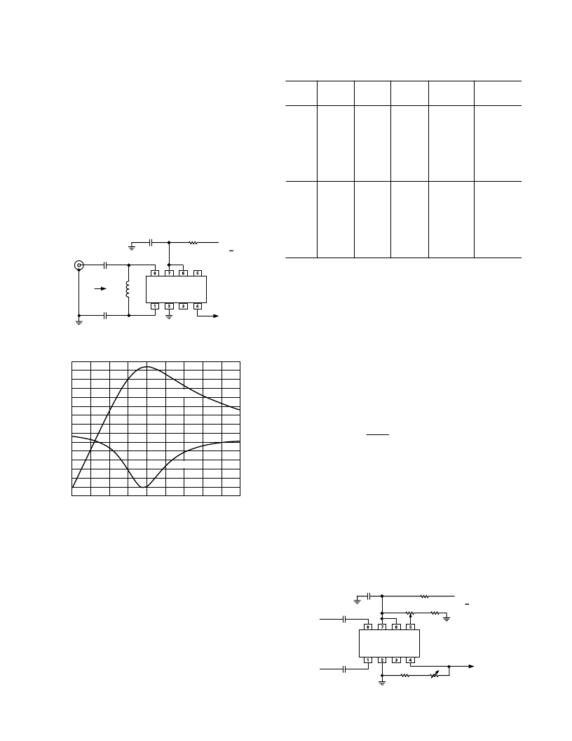
Narrow-Band Matching
T ransformer coupling is useful in broadband applications. How-
ever, a magnetically-coupled transformer may not be convenient
in some situations. At high frequencies, it is often preferable to
use a narrow-band matching network, as shown in Figure 33.
T his has several advantages. T he same voltage gain is achieved,
providing increased sensitivity, but now a measure of selectively
is also introduced. T he component count is low: two capacitors
and an inexpensive chip inductor. Further, by making these
capacitors unequal the amplitudes at INP and INM may be
equalized when driving from a single-sided source; that is, the
network also serves as a balun. Figure 34 shows the response for
a center frequency of 100 MHz; note the very high attenuation
at low frequencies. T he high-frequency attenuation is due to the
input capacitance of the log amp.
INP VPS ENB INT
AD8307
INM COM OFS OUT
C2
50
V
INPUT
–88dBm TO
+3dBm
L
M
C1
4.7
V
NC
NC
0.1
m
F
V
P
, 2.7V – 5.5V
AT 8mA
OUTPUT
25mV/dB
NC = NO CONNECT
Z
IN
= 50
V
Figure 33. High Frequency Input Matching Network
FREQUENCY – MHz
14
13
12
11
10
4
3
2
1
0
–1
60
150
80
D
100
110
130
70
90
120
140
INPUT
GAIN
9
8
7
6
5
Figure 34. Response of 100 MHz Matching Network
T able I provides solutions for a variety of center frequencies F
C
and matching impedances Z
IN
of nominally 50
and 100
.
T he unequal capacitor values were chosen to provide a well-
balanced differential drive, and also to allow better centering of
the frequency response peak when using standard value compo-
nents; this generally results in a Z
IN
that is not exact. T he full
AD8307 HF input impedance and the inductor losses were
included in the modeling.
T able I. Narrow-Band Matching Values
F
C
MHz
10
20
50
100
150
200
250
500
10
20
50
100
150
200
250
500
Z
IN
45
44
46
50
57
57
50
54
103
102
99
98
101
95
92
114
C1
pF
160
82
30
15
10
7.5
6.2
3.9
100
51
22
11
7.5
5.6
4.3
2.2
C2
pF
150
75
27
13
8.2
6.8
5.6
3.3
91
43
18
9.1
6.2
4.7
3.9
2.0
L
M
nH
3300
1600
680
330
220
150
100
39
5600
2700
1000
430
260
180
130
47
Voltage
Gain (dB)
13.3
13.4
13.4
13.4
13.2
12.8
12.3
10.9
10.4
10.4
10.6
10.5
10.3
10.3
9.9
6.8
Slope and Intercept Adjustments
Where higher calibration accuracy is needed, the adjustments
shown in Figure 35 can be used, either singly or in combination.
T he log slope is lowered to 20 mV/dB by shunting the nominally
12.5 k
on-chip load resistor (see Figure 29) with 50 k
,
adjusted by VR1. T he calibration range is
±
10% (18 mV/dB to
22 mV/dB), including full allowance for the variability in the
value of the internal load. T he adjustment may be made by
alternately applying two input levels, provided by an accurate
signal generator, spaced over the central portion of the log amp’s
dynamic range, for example –60 dBm and 0 dBm. An AM-
modulated signal, at the center of the dynamic range, can also
be used. For a modulation depth M, expressed as a fraction, the
decibel range between the peaks and troughs over one cycle of
the modulation period is given by:
dB
=
20 log
10
1
+
M
1
M
For example, using an rms signal level of –40 dBm with a 70%
modulation depth (M = 0.7), the decibel range is 15 dB, as the
signal varies from –47.5 dBm to –32.5 dBm.
T he log intercept is adjustable over a
±
3 dB range, which is
sufficient to absorb the worst-case intercept error in the AD8307
plus some system-level errors. For greater range, set R
S
to zero.
VR2 is adjusted while applying an accurately known CW signal
near the lower end of the dynamic range, in order to minimize
the effect of any residual uncertainty in the slope. For example,
to position the intercept to –80 dBm, a test level of –65 dBm
may be applied and VR2 adjusted to produce a dc output of
15 dB above zero at 25 mV/dB, which is +0.3 V.
(7)
INP VPS ENB INT
AD8307
INM COM OFS OUT
C2 = C
C
INPUT
–75dBm TO
+16dBm
R
S
C1 = C
C
4.7
V
6
3dB
NC
0.1
m
F
V
P
, 2.7V – 5.5V
AT 8mA
20mV/dB
6
10%
VR2
50k
V
32.4k
V
VR1
50k
V
FOR V
P
= 3V, R
S
= 20k
V
V
P
= 5V, R
S
= 51k
V
NC = NO CONNECT
Figure 35. Slope and Intercept Adjustments
相關PDF資料 |
PDF描述 |
|---|---|
| AD8307 | Low Cost DC-500 MHz, 92 dB Logarithmic Amplifier(對數放大器) |
| AD8309ARU-REEL | 5 MHz.500 MHz 100 dB Demodulating Logarithmic Amplifier with Limiter Output |
| AD8309-EVAL | 5 MHz.500 MHz 100 dB Demodulating Logarithmic Amplifier with Limiter Output |
| AD8309ARU | 5 MHz.500 MHz 100 dB Demodulating Logarithmic Amplifier with Limiter Output |
| AD8309ARU-REEL7 | 5 MHz.500 MHz 100 dB Demodulating Logarithmic Amplifier with Limiter Output |
相關代理商/技術參數 |
參數描述 |
|---|---|
| AD8307AR-REEL7 | 功能描述:IC LOGARITHMIC AMP 8-SOIC RoHS:否 類別:集成電路 (IC) >> 線性 - 放大器 - 專用 系列:- 產品培訓模塊:Lead (SnPb) Finish for COTS Obsolescence Mitigation Program 標準包裝:60 系列:- 類型:可變增益放大器 應用:CATV 安裝類型:表面貼裝 封裝/外殼:20-WQFN 裸露焊盤 供應商設備封裝:20-TQFN-EP(5x5) 包裝:托盤 |
| AD8307ARZ | 功能描述:IC LOGARITHMIC AMP 92DB 8-SOIC RoHS:是 類別:集成電路 (IC) >> 線性 - 放大器 - 專用 系列:- 產品培訓模塊:Lead (SnPb) Finish for COTS Obsolescence Mitigation Program 標準包裝:60 系列:- 類型:可變增益放大器 應用:CATV 安裝類型:表面貼裝 封裝/外殼:20-WQFN 裸露焊盤 供應商設備封裝:20-TQFN-EP(5x5) 包裝:托盤 |
| AD8307ARZ | 制造商:Analog Devices 功能描述:Logarithmic Amplifier IC |
| AD8307ARZ-REEL | 功能描述:IC AMP LOGARITHMIC 8SOIC RoHS:是 類別:集成電路 (IC) >> 線性 - 放大器 - 專用 系列:- 產品培訓模塊:Lead (SnPb) Finish for COTS Obsolescence Mitigation Program 標準包裝:60 系列:- 類型:可變增益放大器 應用:CATV 安裝類型:表面貼裝 封裝/外殼:20-WQFN 裸露焊盤 供應商設備封裝:20-TQFN-EP(5x5) 包裝:托盤 |
| AD8307ARZ-RL7 | 功能描述:IC AMP LOGARITHMIC 8-SOIC RoHS:是 類別:集成電路 (IC) >> 線性 - 放大器 - 專用 系列:- 產品培訓模塊:Lead (SnPb) Finish for COTS Obsolescence Mitigation Program 標準包裝:60 系列:- 類型:可變增益放大器 應用:CATV 安裝類型:表面貼裝 封裝/外殼:20-WQFN 裸露焊盤 供應商設備封裝:20-TQFN-EP(5x5) 包裝:托盤 |
發布緊急采購,3分鐘左右您將得到回復。