- 您現在的位置:買賣IC網 > PDF目錄373943 > AD8313ARM-REEL (ANALOG DEVICES INC) 0.1 GHz-2.5 GHz, 70 dB Logarithmic Detector/Controller PDF資料下載
參數資料
| 型號: | AD8313ARM-REEL |
| 廠商: | ANALOG DEVICES INC |
| 元件分類: | 模擬信號調理 |
| 英文描述: | 0.1 GHz-2.5 GHz, 70 dB Logarithmic Detector/Controller |
| 中文描述: | SPECIALTY ANALOG CIRCUIT, PDSO8 |
| 封裝: | MO-187AA, MSOP-8 |
| 文件頁數: | 12/16頁 |
| 文件大小: | 261K |
| 代理商: | AD8313ARM-REEL |
AD8313
–12–
REV. B
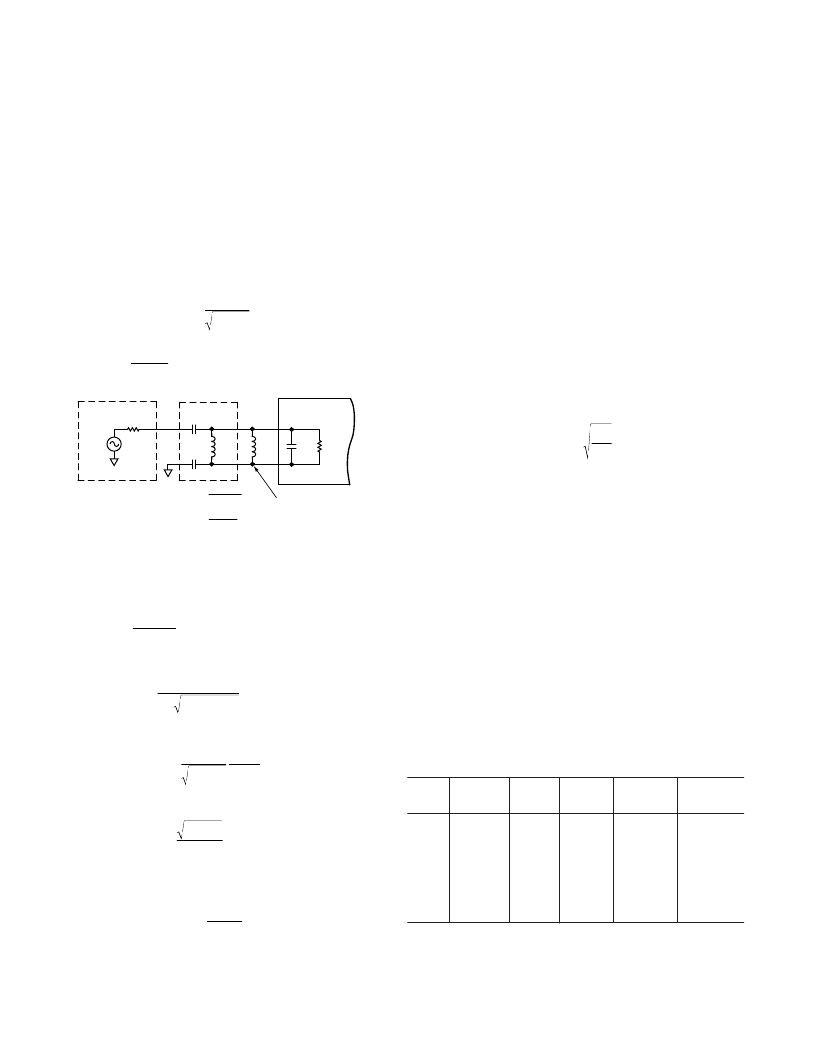
Typically, the AD8313 will need to be matched to 50
. The
input impedance of the AD8313 at 100 MHz can be read from
the Smith Chart (Figure 24) and corresponds to a resistive input
impedance of 900
in parallel with a capacitance of 1.1 pF.
To make the matching process simpler, the input capacitance of
the AD8313, C
IN
, can be temporarily removed from the calcula-
tion by adding a virtual shunt inductor (L
2
), which will resonate
away C
IN
(Figure 34). This inductor will be factored back into
the calculation later. This allows the main calculation to be
based on a simple resistive-to-resistive match (i.e., 50
to
900
).
The resonant frequency is defined by the equation
ω =
1
2
L C
IN
therefore:
L
2
=
1
2
ω
C
IN
= 2.3
μ
H
C
MATCH
=(C1 +
C2)
C2)
L
MATCH
=(L
1
L
2
)
(L
1
+
L
2
)
C1
C2
C
IN
R
IN
AD8313
50
V
50
V
SOURCE
L
1
L
2
TEMPORARY
INDUCTANCE
Figure 34. Input Matching Example
With C
IN
and L
2
temporarily out of the picture, the focus is now
on matching a 50
source resistance to a (purely resistive) load
of 900
and calculating values for C
MATCH
and L
1
.
When
R R
L
C
IN
MATCH
=
1
the input will look purely resistive at a frequency given by
f
L C
O
MATCH
=
1
2
π
= 100 MHz
Solving for
C
MATCH
gives
C
R R
f
pF
MATCH
IN
O
=
=
1
1
2
7 5
.
π
Solving for
L
1
gives
L
R R
2
π
f
IN
O
1
=
= 337.6
nH
Because
L
1
and
L
2
are in parallel, they can be combined to give
the final value for
L
MATCH
(i.e.)
L
L L
L
1
L
MATCH
=
+
2
2
= 294
nH
C1 and C2 can be chosen in a number of ways. First C2 can be
set to a large value such as 1000 pF, so that it appears as an RF
short. C1 would then be set equal to the calculated value of
C
MATCH
. Alternatively, C1 and C2 can each be set to twice
C
MATCH
so that the total series capacitance is equal to C
MATCH
.
By making C1 and C2 slightly unequal (i.e., select C2 to be
about 10% less than C1) but keeping their series value the
same, the amplitude of the signals on INHI and INLO can be
equalized so that the AD8313 is driven in a more balanced
manner. Any one of the three options detailed above can be
used as long as the combined series value of C1 and C2 (i.e.,
C1
×
C2/(C1 + C2)) is equal to C
MATCH
.
In all cases, the values of C
MATCH
and L
MATCH
must be chosen
from standard values. At this point, these values need now be
installed on the board and measured for performance at 100 MHz.
Because of board and layout parasitics, the component values
from the above example had to be tuned to the final values of
C
MATCH
= 8.9 pF and L
MATCH
= 270 nH shown in Table I.
Assuming a lossless matching network and noting conservation
of power, the impedance transformation from R
S
to R
IN
(50
to 900
) has an associated voltage gain given by
Gain
R
R
dB
IN
S
=
20 log
= 12.6
dB
Because the AD8313 input responds to
voltage
and not true
power, the voltage gain of the matching network will increase
the effective input low-end power sensitivity by this amount.
Thus, in this case, the dynamic range will be shifted down-
wards, that is, the 12.6 dB voltage gain will shift the 0 dBm to
–65 dBm input range downwards to –12.6 dBm to –77.6 dBm.
However, because of network losses this gain will not be fully
realized in practice. Reference Figures 31 and 32 for an example
of practical attainable voltage gains.
Table I shows recommended values for the inductor and capaci-
tors in Figure 32 for some selected RF frequencies along with the
associated theoretical voltage gain. These values for a reactive
match are optimal for the board layout detailed as Figure 45.
As previously discussed, a modification of the board layout will
produce networks that may not perform as specified. At 2.5 GHz, a
shunt inductor is sufficient to achieve match. Consequently, C1
and C2 are set sufficiently high that they appear as RF shorts.
Table I. Recommended Values for C1, C2 and L
MATCH
in
Figure 33
F
req.
(MHz)
C
MATCH
(pF)
C1
(pF)
C2
(pF)
L
MATCH
(nH)
Voltage
Gain (dB)
100
8.9
22
9
3
1.5
3
1.5
390
15
1000
3
1000
3
1000
390
270
270
8.2
8.2
2.2
2.2
2.2
12.6
900
1.5
9.0
1900
1.5
6.2
2500
Large
3.2
Figure 35 shows the voltage response of the 100 MHz matching
network; note the high attenuation at lower frequencies typical
of a high-pass network.
相關PDF資料 |
PDF描述 |
|---|---|
| AD8313-EVAL | 0.1 GHz-2.5 GHz, 70 dB Logarithmic Detector/Controller |
| AD8313 | 0.1 GHz-2.5 GHz,70dB Logarithmic Detector/Controller(頻率為0.1 GHz-2.5 GHz,增益為70dB的對數檢測器/控制器) |
| AD8314ARM | 100 MHz-2500 MHz 45 dB RF Detector/Controller |
| AD8314ARM-REEL | 100 MHz-2500 MHz 45 dB RF Detector/Controller |
| AD8314ARM-REEL7 | 100 MHz-2500 MHz 45 dB RF Detector/Controller |
相關代理商/技術參數 |
參數描述 |
|---|---|
| AD8313ARM-REEL7 | 功能描述:IC LOG DETECTOR/CTRLR 8-MSOP RoHS:否 類別:RF/IF 和 RFID >> RF 檢測器 系列:- 產品變化通告:Product Discontinuation 15/May/2006 標準包裝:3,000 系列:- 頻率:100MHz ~ 2GHz RF 型:手機,GSM,DCS,PCS 輸入范圍:- 精確度:- 電源電壓:2.7 V ~ 5.5 V 電流 - 電源:300µA 包裝:帶卷 (TR) 封裝/外殼:SC-74,SOT-457 其它名稱:NCS5000SNT1GOS |
| AD8313ARMZ | 功能描述:IC LOGARTIHMIC AMP 70DB 8-MSOP RoHS:是 類別:RF/IF 和 RFID >> RF 檢測器 系列:- 產品變化通告:Product Discontinuation 15/May/2006 標準包裝:3,000 系列:- 頻率:100MHz ~ 2GHz RF 型:手機,GSM,DCS,PCS 輸入范圍:- 精確度:- 電源電壓:2.7 V ~ 5.5 V 電流 - 電源:300µA 包裝:帶卷 (TR) 封裝/外殼:SC-74,SOT-457 其它名稱:NCS5000SNT1GOS |
| AD8313ARMZ | 制造商:Analog Devices 功能描述:IC DETECTOR/CONTROLLER 制造商:Analog Devices 功能描述:IC, DETECTOR/CONTROLLER |
| AD8313ARMZ | 制造商:Analog Devices 功能描述:IC, RF LOG DET, 100kHz to 2.5GHz, MSOP-8 |
| AD8313ARMZ-REEL | 功能描述:IC LOG DETECTOR/CTRLR 8MSOP RoHS:是 類別:RF/IF 和 RFID >> RF 檢測器 系列:- 產品變化通告:Product Discontinuation 15/May/2006 標準包裝:3,000 系列:- 頻率:100MHz ~ 2GHz RF 型:手機,GSM,DCS,PCS 輸入范圍:- 精確度:- 電源電壓:2.7 V ~ 5.5 V 電流 - 電源:300µA 包裝:帶卷 (TR) 封裝/外殼:SC-74,SOT-457 其它名稱:NCS5000SNT1GOS |
發布緊急采購,3分鐘左右您將得到回復。