- 您現在的位置:買賣IC網 > PDF目錄373944 > AD8332ARU (ANALOG DEVICES INC) Ultralow Noise VGAs with Preamplifier and Programmable RIN PDF資料下載
參數資料
| 型號: | AD8332ARU |
| 廠商: | ANALOG DEVICES INC |
| 元件分類: | 消費家電 |
| 英文描述: | Ultralow Noise VGAs with Preamplifier and Programmable RIN |
| 中文描述: | SPECIALTY CONSUMER CIRCUIT, PDSO28 |
| 封裝: | MO-153AE, TSSOP-28 |
| 文件頁數: | 24/32頁 |
| 文件大小: | 482K |
| 代理商: | AD8332ARU |
第1頁第2頁第3頁第4頁第5頁第6頁第7頁第8頁第9頁第10頁第11頁第12頁第13頁第14頁第15頁第16頁第17頁第18頁第19頁第20頁第21頁第22頁第23頁當前第24頁第25頁第26頁第27頁第28頁第29頁第30頁第31頁第32頁
AD8331/AD8332
Table 4. Clamp Resistor Values
Clamp Level
(V p-p)
Rev. C | Page 24 of 32
Clamp Resistor Value (k)
HILO = LO
1.21
2.74
4.75
7.5
11
16.9
26.7
49.9
100
HILO = HI
2.21
4.02
6.49
9.53
14.7
23.2
39.2
73.2
0.5
1.0
1.5
2.0
2.5
3.0
3.5
4.0
4.4
Output Filtering and Series Resistor
Requirements
To ensure stability at the high end of the gain control range,
series resistors or ferrite beads are recommended for the
outputs when driving large capacitive loads, or circuits on other
boards,. These components can be part of the external
noise filter.
Recommended resistor values are 84.5 for LO gain mode and
100 for HI gain mode (see Figure 66) and are placed near
Pins VOH and VOL. Lower value resistors are permissible for
applications with nearby loads or with gains less than 40 dB.
Lower values are best selected empirically.
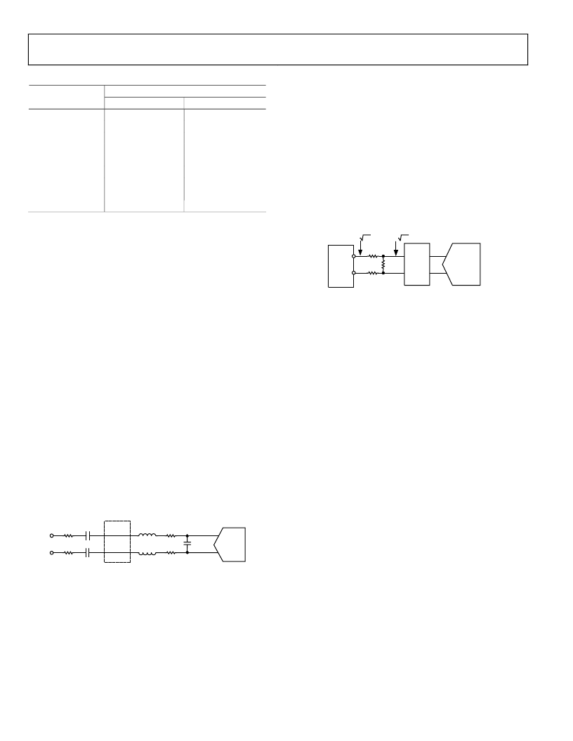
An antialiasing noise filter is typically used with an ADC. Filter
requirements are application dependent.
When the ADC resides on a separate board, the majority of
filter components should be placed nearby to suppress noise
picked up between boards and mitigates charge kickback from
the ADC inputs. Any series resistance beyond that required for
output stability should be placed on the ADC board. Figure 70
shows a second order low-pass filter with a bandwidth of
20 MHz. The capacitor is chosen in conjunction with the 10 pF
input capacitance of the ADC.
18pF
OPTIONAL
BACKPLANE
84.5
0.1
μ
F
0.1
μ
F
1.5
μ
H
1.5
μ
H
158
158
84.5
ADC
Figure 70. 20 MHz Second-Order Low-Pass Filter
DRIVING ADCS
The output drive will accommodate a wide range of ADCs. The
noise floor requirements of the VGA will depend on a number
of application factors, including bit resolution, sampling rate,
full-scale voltage, and the bandwidth of the noise/antialias filter.
The output noise floor and gain range can be adjusted by
selecting HI or LO gain mode.
The relative noise and distortion performance of the two gain
modes can be compared in Figure 21 and Figure 27 through
Figure 37. The 48 nV/√Hz noise floor of the LO gain mode is
suited to converters with higher sampling rates or resolutions
(such as 12 bits). Both gain modes can accommodate ADC full-
scale voltages as high as 4 V p-p. Since distortion performance
remains favorable for output voltages as high as 4 V p-p (see
Figure 32), it is possible to lower the output-referred noise even
further by using a resistive attenuator (or transformer) at the
output. The circuit in Figure 71 has an output full-scale range of
2 V p-p, a gain range of –10.5 dB to +37.5 dB, and an output
noise floor of 24 nV/√Hz, making it suitable for some 14-bit
ADC applications.
VOH
VOL
LPF
4V p-p DIFF,
48n V/
187
2V p-p DIFF,
24n V/
2:1
374
HZ
187
ADC
AD6644
HZ
0
Figure 71. Adjusting the Noise Floor for 14-Bit ADCs
OVERLOAD
These devices respond gracefully to large signals that overload
its input stage and to normal signals that overload the VGA
when the gain is set unexpectedly high. Each stage is designed
for clean-limited overload waveforms and fast recovery when
gain setting or input amplitude is reduced.
Signals larger than ±275 mV at the LNA input are clipped to
5 V p-p differential prior to the input of the VGA. Figure 44
shows the response to a 1 V p-p input burst. The symmetric
overload waveform is important for applications, such as CW
Doppler ultrasound, where the spectrum of the LNA outputs
during overload is critical. The input stage is also designed to
accommodate signals as high as ±2.5 V without triggering the
slow-settling ESD input protection diodes.
Both stages of the VGA are susceptible to overload. Postamp
limiting is more common and results in the clean-limited
output characteristics found in Figure 45. Under more extreme
conditions, the X-AMP will overload, causing the minor glitches
evident in Figure 46. Recovery is fast in all cases. The graph in
Figure 72 summarizes the combinations of input signal and
gain that lead to the different types of overload.
相關PDF資料 |
PDF描述 |
|---|---|
| AD8331ARQ-REEL | Ultralow Noise VGAs with Preamplifier and Programmable RIN |
| AD8331ARQ-REEL7 | Ultralow Noise VGAs with Preamplifier and Programmable RIN |
| AD8341 | 1.5 GHz to 2.4 GHz RF Vector Modulator |
| AD8341-EVAL | 1.5 GHz to 2.4 GHz RF Vector Modulator |
| AD8341ACPZ-REEL72 | 1.5 GHz to 2.4 GHz RF Vector Modulator |
相關代理商/技術參數 |
參數描述 |
|---|---|
| AD8332ARU-REEL | 功能描述:IC VGA DUAL W/PREAMP LN 28-TSSOP RoHS:否 類別:集成電路 (IC) >> 線性 - 放大器 - 專用 系列:X-AMP® 產品培訓模塊:Lead (SnPb) Finish for COTS Obsolescence Mitigation Program 標準包裝:60 系列:- 類型:可變增益放大器 應用:CATV 安裝類型:表面貼裝 封裝/外殼:20-WQFN 裸露焊盤 供應商設備封裝:20-TQFN-EP(5x5) 包裝:托盤 |
| AD8332ARU-REEL7 | 功能描述:IC VGA DUAL W/PREAMP LN 28-TSSOP RoHS:否 類別:集成電路 (IC) >> 線性 - 放大器 - 專用 系列:X-AMP® 產品培訓模塊:Lead (SnPb) Finish for COTS Obsolescence Mitigation Program 標準包裝:60 系列:- 類型:可變增益放大器 應用:CATV 安裝類型:表面貼裝 封裝/外殼:20-WQFN 裸露焊盤 供應商設備封裝:20-TQFN-EP(5x5) 包裝:托盤 |
| AD8332ARUZ | 功能描述:IC VGA DUAL W/PREAMP LN 28-TSSOP RoHS:是 類別:集成電路 (IC) >> 線性 - 放大器 - 專用 系列:X-AMP® 產品培訓模塊:Lead (SnPb) Finish for COTS Obsolescence Mitigation Program 標準包裝:60 系列:- 類型:可變增益放大器 應用:CATV 安裝類型:表面貼裝 封裝/外殼:20-WQFN 裸露焊盤 供應商設備封裝:20-TQFN-EP(5x5) 包裝:托盤 |
| AD8332ARUZ | 制造商:Analog Devices 功能描述:IC PRE-AMP ULTRA LOW NOISE |
| AD8332ARUZ-R7 | 功能描述:IC AMP VAR GAIN 2CHAN 28TSSOP RoHS:是 類別:集成電路 (IC) >> 線性 - 放大器 - 專用 系列:X-AMP® 產品培訓模塊:Lead (SnPb) Finish for COTS Obsolescence Mitigation Program 標準包裝:60 系列:- 類型:可變增益放大器 應用:CATV 安裝類型:表面貼裝 封裝/外殼:20-WQFN 裸露焊盤 供應商設備封裝:20-TQFN-EP(5x5) 包裝:托盤 |
發布緊急采購,3分鐘左右您將得到回復。