- 您現在的位置:買賣IC網 > PDF目錄373944 > AD8343ARU-REEL7 (ANALOG DEVICES INC) DC-to-2.5 GHz High IP3 Active Mixer PDF資料下載
參數資料
| 型號: | AD8343ARU-REEL7 |
| 廠商: | ANALOG DEVICES INC |
| 元件分類: | 衰減器 |
| 英文描述: | DC-to-2.5 GHz High IP3 Active Mixer |
| 中文描述: | 0 MHz - 2500 MHz RF/MICROWAVE DOUBLE BALANCED MIXER |
| 封裝: | PLASTIC, TSSOP-14 |
| 文件頁數: | 19/27頁 |
| 文件大小: | 394K |
| 代理商: | AD8343ARU-REEL7 |
第1頁第2頁第3頁第4頁第5頁第6頁第7頁第8頁第9頁第10頁第11頁第12頁第13頁第14頁第15頁第16頁第17頁第18頁當前第19頁第20頁第21頁第22頁第23頁第24頁第25頁第26頁第27頁
REV. 0
AD8343
–19–
The idea is to make a differential measurement at the output of
the balun, with the single-ended port of the balun terminated in
50
. Again, there are two methods available for making this
measurement: use of the ATN Multiport Network Analyzer to
measure the differential impedance directly, or use of a standard
two-port network analyzer and Konstroffer
’
s transformation
equation.
In order to utilize a standard two-port analyzer, connect the two
ports of the calibrated vector network analyzer (VNA) to the
balanced output pins of the balun, measure the two-port S
parameters, then use Konstroffer
’
s formula to convert the two-
port parameters to one-port differential
Γ
.
(
(
Step 3: Measure AD8343 Differential Impedance at Location
of First Matching Component
Once the target impedance is established, the next step in
matching to the AD8343 is to measure the differential imped-
ance at the location of the first matching component. The
“
A
”
side of the evaluation board is designed to facilitate doing so.
Before doing the board measurements, it is necessary to perform
a full two-port calibration of the VNA at the ends of the cables
that will be used to connect to the board
’
s input connectors,
using the SOLT (Short, Open, Load, Thru) method or equiva-
lent. It is a good idea to set the VNA
’
s sweep span to a few
hundred MHz or more for this work because it is often useful to
see what the circuit is doing over a large range of frequencies,
not just at the intended operating frequency. This is particularly
useful for detecting stability problems.
After the calibration is completed, connect network analyzer
ports one and two to the differential inputs of the AD8343
Evaluation Board.
On the AD8343 Evaluation Board, it is necessary to temporarily
install jumpers at Z1A and Z3A if Z4A is the desired component
location. Zero ohm resistors or capacitors of sufficient value
to exhibit negligible reactance work nicely for this purpose.
Next, extend the reference plane to the location of your first
matching component. This is accomplished by solidly shorting
both pads at the component location to GND (
Note: Power to the
board must be OFF for this operation!
) Adjust the VNA reference
plane extensions to make the entire trace collapse to a point (or
best approximation thereof near the desired frequency) at the
zero impedance point of the Smith Chart. Do this for each port.
A reasonable way to provide a good RF short is to solder a piece
of thin copper or brass sheet on edge across the pads to the nearby
GND pads.
Now, remove the short, apply power to the board, and take
readings. Take a look at both S11 and S22 to verify that they
remain inside the unit circle of the Smith Chart over the whole
frequency range being swept. If they fail to do so, this is a sign
that the device is unstable (perhaps due to an inappropriate
common-mode load) or that the network analyzer calibration is
wrong. Either way the problem must be addressed before pro-
ceeding further.
Assuming that the values look reasonable, use Konstroffer
’
s
formula to convert to differential
Γ
.
Γ
s
S
S
S
S
S
S
S
S
S
S
S
S
S
S
=
×
)
+
12
(
(
+
(
×
(
)
)
+
)
+
)
2
11
21 1
22
12
1
11
21 1
22
2
12
2
21 1
22
1
11
21 1
22
Step 4: Design the Matching Network
The next step is to perform a trial design of a matching network
utilizing standard impedance matching techniques. The network
may be designed using single-ended network values, then con-
verted to differential form as illustrated in Figure 8. Figure 19
shows a theoretical design of a series C/shunt C
“
L
”
network
applied between 50
and a typical load at 1.8 GHz.
0.2
0.5
1.0
2.9pF SHUNT CAPACITOR
5.0
Figure 19. Theoretical Design of Matching Network
This theoretical design is important because it establishes the
basic topology and the initial matching value for the network.
The theoretical value of 2.9 pF for the initial matching com-
ponent is not available in standard capacitor values, so a 3.0 pF
is placed in the first shunt matching location. This value may
prove to be too large, causing an overshoot of the 50
real imped-
ance circle, or too small, causing the opposite effect. Always keep
in mind that this is a measure of
differential
impedance. The value
of the capacitor should be modified to achieve the desired 50
real impedance.
However, it may occasionally happen that the inserted shunt
capacitor moves the impedance in completely unexpected and
undesired ways. This is almost always an indication that the
reference plane was improperly extended for the measurement.
The user should readjust the reference planes and attempt the
shunt capacitor match with another calculated value.
When a differential impedance of 50
(real part) is achieved,
the board should be deenergized and another short placed on
the board in preparation for resetting the port extensions to a
new reference plane location. This short should be placed where
next the series components are expected to be added, and it is
important that both ports one and two be extended to this point
on the board.
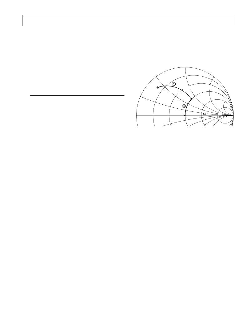
Another differential measurement must be taken at this point to
establish the starting impedance value for the next matching
component. Note that if 50
PCB traces of finite length are
used to connect pads, the impedance will experience an angular
rotation to another location on the Smith Chart as indicated in
Figure 20.
相關PDF資料 |
PDF描述 |
|---|---|
| AD8344 | Active Receive Mixer 400 MHz to 1.2 GHz |
| AD8344-EVAL | Active Receive Mixer 400 MHz to 1.2 GHz |
| AD8344ACPZ-REEL7 | Active Receive Mixer 400 MHz to 1.2 GHz |
| AD8344ACPZ-WP | Active Receive Mixer 400 MHz to 1.2 GHz |
| AD8345ARE-REEL | 250 MHz.1000 MHz Quadrature Modulator |
相關代理商/技術參數 |
參數描述 |
|---|---|
| AD8343ARUZ | 功能描述:IC MIXER ACTIVE HI-IP3 14-TSSOP RoHS:是 類別:RF/IF 和 RFID >> RF 混頻器 系列:AD8343 產品培訓模塊:Lead (SnPb) Finish for COTS Obsolescence Mitigation Program 標準包裝:100 系列:- RF 型:W-CDMA 頻率:2.11GHz ~ 2.17GHz 混頻器數目:1 增益:17dB 噪音數據:2.2dB 次要屬性:- 電流 - 電源:11.7mA 電源電壓:2.7 V ~ 3.3 V 包裝:托盤 封裝/外殼:12-VFQFN 裸露焊盤 供應商設備封裝:12-QFN-EP(3x3) |
| AD8343ARUZ | 制造商:Analog Devices 功能描述:IF Subsystem |
| AD8343ARUZ-REEL | 功能描述:IC MIXER ACTIVE HIGH IP3 14TSSOP RoHS:是 類別:RF/IF 和 RFID >> RF 混頻器 系列:AD8343 產品培訓模塊:Lead (SnPb) Finish for COTS Obsolescence Mitigation Program 標準包裝:100 系列:- RF 型:W-CDMA 頻率:2.11GHz ~ 2.17GHz 混頻器數目:1 增益:17dB 噪音數據:2.2dB 次要屬性:- 電流 - 電源:11.7mA 電源電壓:2.7 V ~ 3.3 V 包裝:托盤 封裝/外殼:12-VFQFN 裸露焊盤 供應商設備封裝:12-QFN-EP(3x3) |
| AD8343ARUZ-REEL7 | 功能描述:IC MIXER ACTIVE HIGH IP3 14TSSOP RoHS:是 類別:RF/IF 和 RFID >> RF 混頻器 系列:AD8343 產品培訓模塊:Lead (SnPb) Finish for COTS Obsolescence Mitigation Program 標準包裝:100 系列:- RF 型:W-CDMA 頻率:2.11GHz ~ 2.17GHz 混頻器數目:1 增益:17dB 噪音數據:2.2dB 次要屬性:- 電流 - 電源:11.7mA 電源電壓:2.7 V ~ 3.3 V 包裝:托盤 封裝/外殼:12-VFQFN 裸露焊盤 供應商設備封裝:12-QFN-EP(3x3) |
| AD8343-EVAL | 制造商:Analog Devices 功能描述:AD8343 EVALUATION BOARD - Bulk |
發布緊急采購,3分鐘左右您將得到回復。