- 您現(xiàn)在的位置:買賣IC網(wǎng) > PDF目錄373944 > AD8344 (Analog Devices, Inc.) Active Receive Mixer 400 MHz to 1.2 GHz PDF資料下載
參數(shù)資料
| 型號(hào): | AD8344 |
| 廠商: | Analog Devices, Inc. |
| 英文描述: | Active Receive Mixer 400 MHz to 1.2 GHz |
| 中文描述: | 有源接收混頻器400 MHz到1.2 GHz的 |
| 文件頁數(shù): | 13/20頁 |
| 文件大小: | 429K |
| 代理商: | AD8344 |
AD8344
CIRCUIT DESCRIPTION
The AD8344 is a down converting mixer optimized for opera-
tion within the input frequency range of 400 MHz to 1.2 GHz. It
has a single-ended, 50 RF input, as well as a single-ended,
50 local oscillator (LO) input. The IF outputs are differential
open collectors. The mixer current can be adjusted by the value
of an external resistor to optimize performance for gain com-
pression and intermodulation or for low power operation.
Figure 35 shows the basic blocks of the mixer, which includes
the LO buffer, RF voltage-to-current converter, bias cell, and
mixing core.
Rev. 0 | Page 13 of 20
e
The RF voltage to RF current conversion is done via an
inductively degenerated differential pair. When one side of the
differential pair is ac grounded, the other input can be driven
single-ended. The RF inputs can also be driven differentially.
The voltage-to-current converter then drives the emitters of a
four-transistor switching core. This switching core is driven by
an amplified version of the local oscillator signal connected to
the LO input. There are three limiting gain stages between the
external LO signal and the switching core. The first stage con-
verts the single-ended LO drive to a well balanced differential
drive. The differential drive then passes through two more gain
stages, which ensures a limited signal drives the switching core.
This affords the user a lower LO drive requirement, while
maintaining excellent distortion and compression performance.
The output signal of these three LO gain stages drives the four
transistors within the mixer core to commutate at the rate of th
local oscillator frequency. The output of the mixer core is taken
directly from these open collectors. The open collector outputs
present a high impedance at the IF frequency. The conversion
gain of the mixer depends directly on the impedance presented
to these open collectors. In characterization, a 200 load was
presented to the part via a 4:1 impedance transformer.
The AD8344 also features a power-down function.
Application of a logic low at the PWDN pin allows normal
operation. A high logic level at the PWDN pin shuts down the
AD8344. Power consumption when the part is disabled is less
than 10 mW.
The bias for the mixer is set with an external resistor from the
EXRB pin to ground. The value of this resistor directly affects
the dynamic range of the mixer. The external resistor should not
be lower than 2.4 k. Permanent damage to the part will result
if values below 2.4 k are used.
0
LO
INPUT
VPLO
IFOP
IFOM
RFIN
VPMX
RFCM
BIAS
EXTERNAL
BIAS
RESISTOR
VPDC
PWDN
SE
TO
DIFF
Figure 35. AD8344 Simplified Schematic
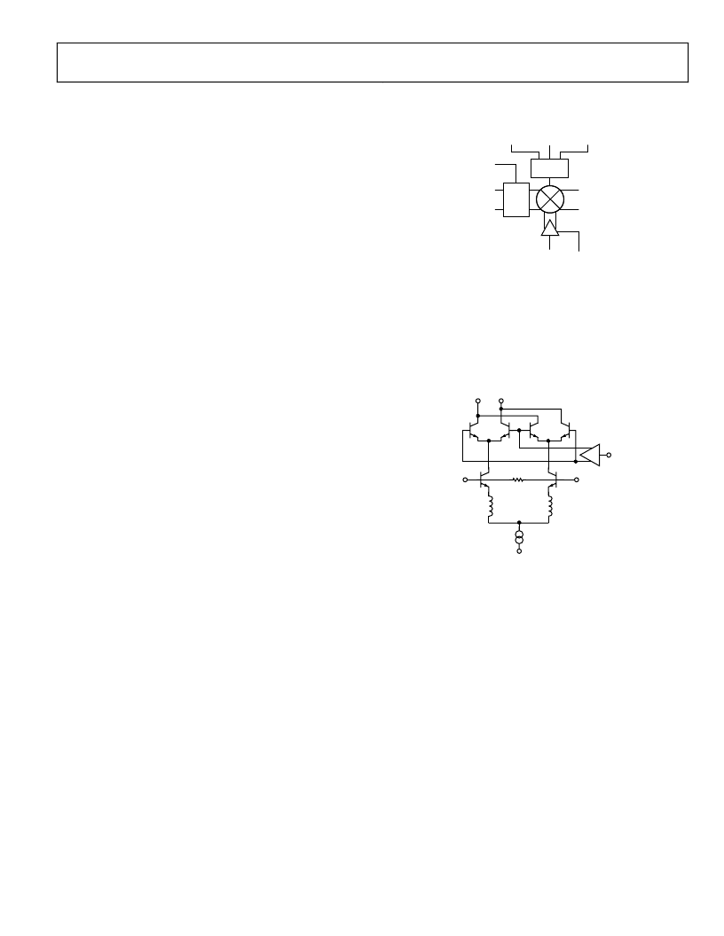
As shown in Figure 36, the IF output pins, IFOP and IFOM, are
directly connected to the open collectors of the NPN transistors
in the mixer core so the differential and single-ended imped-
ances looking into this port are relatively high, on the order of
several k. A connection between the supply voltage and these
output pins is required for proper mixer core operation.
0
IFOP IFOM
LOIN
RFCM
RFIN
COMM
Figure 36. Mixer Core Simplified Schematic
The AD8344 has three pins for the supply voltage: VPDC,
VPMX, and VPLO. These pins are separated to minimize or
eliminate possible parasitic coupling paths within the AD8344
that could cause spurious signals or reduced interport isolation.
Consequently, each of these pins should be well bypassed and
decoupled as close to the AD8344 as possible.
相關(guān)PDF資料 |
PDF描述 |
|---|---|
| AD8344-EVAL | Active Receive Mixer 400 MHz to 1.2 GHz |
| AD8344ACPZ-REEL7 | Active Receive Mixer 400 MHz to 1.2 GHz |
| AD8344ACPZ-WP | Active Receive Mixer 400 MHz to 1.2 GHz |
| AD8345ARE-REEL | 250 MHz.1000 MHz Quadrature Modulator |
| AD8345ARE-REEL7 | 250 MHz.1000 MHz Quadrature Modulator |
相關(guān)代理商/技術(shù)參數(shù) |
參數(shù)描述 |
|---|---|
| AD8344ACPZ | 制造商:Analog Devices 功能描述:UP/DOWN CONV MIXER 5V 1.2GHZ 16LFCSP EP - Tape and Reel 制造商:Analog Devices 功能描述:IC SM RF MIXER 800MHZ |
| AD8344ACPZ | 制造商:Analog Devices 功能描述:IC RF MIXER 800MHZ SMD LFCSP-16 |
| AD8344ACPZ-REEL7 | 功能描述:IC MIXER 400MHZ-1.2GHZ 16-LFCSP RoHS:是 類別:RF/IF 和 RFID >> RF 混頻器 系列:AD8344 產(chǎn)品培訓(xùn)模塊:Lead (SnPb) Finish for COTS Obsolescence Mitigation Program 標(biāo)準(zhǔn)包裝:100 系列:- RF 型:W-CDMA 頻率:2.11GHz ~ 2.17GHz 混頻器數(shù)目:1 增益:17dB 噪音數(shù)據(jù):2.2dB 次要屬性:- 電流 - 電源:11.7mA 電源電壓:2.7 V ~ 3.3 V 包裝:托盤 封裝/外殼:12-VFQFN 裸露焊盤 供應(yīng)商設(shè)備封裝:12-QFN-EP(3x3) |
| AD8344ACPZ-WP | 制造商:Analog Devices 功能描述:UP/DOWN CONV MIXER 5V 1.2GHZ 16LFCSP EP - Waffle Pack |
| AD8344-EVAL | 制造商:Analog Devices 功能描述:Evaluation Kit For Active Receive Mixer 制造商:Analog Devices 功能描述:EVAL KIT FOR ACTV RECEIVE MIXER - Bulk |
發(fā)布緊急采購(gòu),3分鐘左右您將得到回復(fù)。