- 您現在的位置:買賣IC網 > PDF目錄373944 > AD8345-EVAL (Analog Devices, Inc.) 250 MHz.1000 MHz Quadrature Modulator PDF資料下載
參數資料
| 型號: | AD8345-EVAL |
| 廠商: | Analog Devices, Inc. |
| 英文描述: | 250 MHz.1000 MHz Quadrature Modulator |
| 中文描述: | 250 MHz.1000兆赫正交調制器 |
| 文件頁數: | 9/16頁 |
| 文件大小: | 372K |
| 代理商: | AD8345-EVAL |
REV. 0
AD8345
–9–
16
15
14
13
12
11
10
9
1
2
3
4
5
6
7
8
AD8345
QBBP
QBBN
COM3
COM3
VPS2
VOUT
COM2
COM3
IBBP
IBBN
COM3
COM1
LOIN
LOIP
VPS1
ENBL
IP
1
T1
ETC1-1-13
2
3
4
5
LO
R1
50
C6
1000pF
C7
1000pF
IN
C3
1000pF
C4
+V
S
QP
QN
C1
1000pF
C2
0.01 F
+V
S
VOUT
C5
1000pF
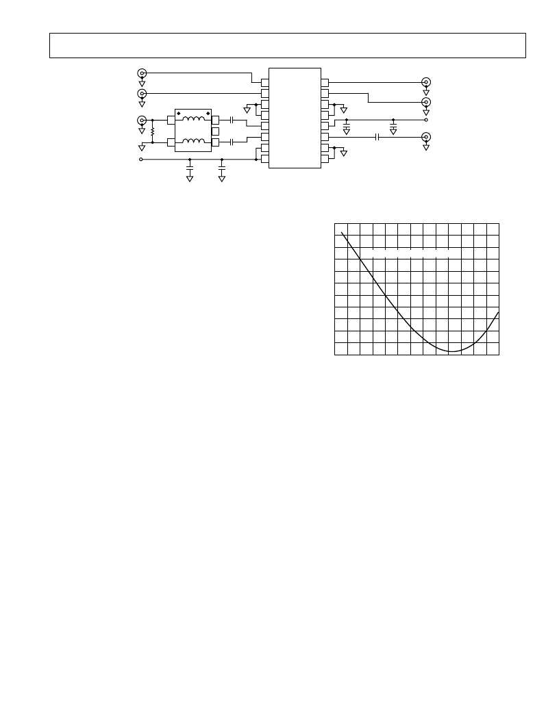
Figure 3. Basic Connections
LO FREQUENCY
–
MHz
40
S
–
–
60
60
80
100 120 140 160 180 200 220 240 260 280 300
–
55
–
50
–
45
–
40
–
35
–
30
–
25
–
20
–
15
–
10
–
5
V
S
= 5V, DIFFERENTIAL INPUT = 1.2V
Figure 4. Typical Lower Frequency Sideband Suppression
Performance
Baseband I and Q Channel Drive
The I and Q channel baseband inputs should be driven differen-
tially. This is convenient as most modern high-speed DACs
have differential outputs. For optimal performance at V
S
= 5 V,
the drive signal should be a 1.2 V p-p differential signal with a
bias level of 0.7 V; that is, each input should swing from 0.4 V
to 1 V. If the AD8345 is being run on a lower supply voltage,
the peak-to-peak voltage on the I and Q channel inputs must be
reduced to avoid input clipping. For example, at a supply volt-
age of 2.7 V, a 200 mV p-p differential drive is recommended.
This will result in a corresponding reduction in output power
(see TPC 1). The I and Q inputs have a large input bandwidth
of approximately 80 MHz. At lower baseband input levels, the
input bandwidth increases (see TPC 2).
If the baseband signal has a high peak-to-average ratio (e.g.,
CDMA or WCDMA), the rms signal strength will have to be
backed off from this peak level in order to prevent clipping of
the signal peaks. Clipping of signal peaks will tend to increase
signal leakage into adjacent channels. Backing off the I and Q
signal strength in the manner recommended will reduce the output
power by a corresponding amount. This also applies to multicarrier
applications where the per-carrier output power will be lower by
3 dB for each doubling of the number of output carriers.
BASIC CONNECTIONS
The basic connections for operating the AD8345 are shown in
Figure 3. A single power supply of between 2.7 V and 5.5 V is
applied to pins VPS1 and VPS2. A pair of ESD protection diodes
are connected internally between VPS1 and VPS2 so these must
be tied to the same potential. Both pins should be individually
decoupled using 1000 pF and 0.01
μ
F capacitors, located as
close as possible to the device. For normal operation, the enable
pin, ENBL, must be pulled high. The turn-on threshold for
ENBL is V
S
/2. Pins COM1 to COM3 should all be tied to the
same low impedance ground plane.
LO Drive
In Figure 3, a 50
resistor to ground combines with the device’s
high input impedance to provide an overall input impedance of
approximately 50
(see TPC 17 for a plot of LO port input
impedance). For maximum LO suppression at the output, a
differential LO drive is recommended. In Figure 3, this is
achieved using a balun (M/A-COM Part Number ETC1-1-13).
The output of the balun is ac coupled to the LO inputs which
have a bias level about 1.8 V dc. An LO drive level of –2 dBm is
recommended for lowest output noise. Higher levels will degrade
linearity while lower levels will tend to increase the noise floor
slightly. For example, reducing the LO power from –2 dBm to
–10 dBm will increase the noise floor by approximately 0.3 dB
(see TPC 19).
The LO terminal can be driven single-ended at the expense of
slightly higher LO leakage. LOIN is ac coupled to ground using
a capacitor and LOIP is driven through a coupling capacitor
from a (single-ended) 50
source (this scheme could also be
reversed with the drive signal being applied to LOIN).
LO Frequency Range
The frequency range on the LO input is limited by the internal
quadrature phase splitter. The phase splitter generates drive
signals for the internal mixers which are 90
°
out of phase relative
to one another. Outside of the specified LO frequency range of
250 MHz to 1 GHz, this quadrature accuracy degrades, result-
ing in decreased sideband suppression. See TPC 9 for a plot of
sideband suppression vs. LO frequency from 250 MHz to 1GHz.
Figure 4 shows the sideband suppression of a typical device
from 50 MHz to 300 MHz. The level of sideband suppression
degradation below 250 MHz will be subject to manufacturing
process variations.
相關PDF資料 |
PDF描述 |
|---|---|
| AD8345ARE | 250 MHz.1000 MHz Quadrature Modulator |
| AD8346ARU-REEL | 0.8 GHz-2.5 GHz Quadrature Modulator |
| AD8346 | 0.8 GHz-2.5 GHz Quadrature Modulator |
| AD8346-EVAL | 0.8 GHz-2.5 GHz Quadrature Modulator |
| AD8346ARU | 0.8 GHz-2.5 GHz Quadrature Modulator |
相關代理商/技術參數 |
參數描述 |
|---|---|
| AD8345-EVALZ | 制造商:Analog Devices 功能描述:EVAL KIT FOR 140 MHZ TO 1000 MHZ QUADRATURE MODULATOR - Bulk |
| AD8346 | 制造商:AD 制造商全稱:Analog Devices 功能描述:300 MHz to 1000 MHz Quadrature Modulator |
| AD8346AF-EMX | 制造商:Analog Devices 功能描述:- Rail/Tube |
| AD8346ARU | 功能描述:IC QUADRATURE MOD .8GHZ 16-TSSOP RoHS:否 類別:RF/IF 和 RFID >> RF 調制器 系列:- 產品培訓模塊:Lead (SnPb) Finish for COTS Obsolescence Mitigation Program 標準包裝:2,500 系列:- 功能:調制器 LO 頻率:700MHz ~ 2.3GHz RF 頻率:700MHz ~ 2.3GHz P1dB:1dBm 底噪:-148dBm/Hz 輸出功率:-1dBm 電流 - 電源:46mA 電源電壓:2.7 V ~ 3.6 V 測試頻率:1.75GHz 封裝/外殼:28-WFQFN 裸露焊盤 包裝:帶卷 (TR) |
| AD8346ARU-REEL | 制造商:Analog Devices 功能描述:Quadrature Mod 70MHz 16-Pin TSSOP T/R 制造商:Analog Devices 功能描述:QUADRATURE MOD 70MHZ 16TSSOP - Tape and Reel 制造商:Rochester Electronics LLC 功能描述:TSSOP DIRECT QUADRATURE MODULATOR - Tape and Reel |
發布緊急采購,3分鐘左右您將得到回復。