- 您現在的位置:買賣IC網 > PDF目錄373944 > AD8345ARE (ANALOG DEVICES INC) 250 MHz.1000 MHz Quadrature Modulator PDF資料下載
參數資料
| 型號: | AD8345ARE |
| 廠商: | ANALOG DEVICES INC |
| 元件分類: | 衰減器 |
| 英文描述: | 250 MHz.1000 MHz Quadrature Modulator |
| 中文描述: | 140 MHz - 1000 MHz RF/MICROWAVE QUADRAPHASE MODULATOR |
| 封裝: | MO-153ABT, TSSOP-16 |
| 文件頁數: | 11/16頁 |
| 文件大小: | 372K |
| 代理商: | AD8345ARE |
REV. 0
AD8345
–11–
Note that this circuit assumes that the single-ended I and Q signals
are ground referenced. Any differential dc-offsets will result
in increased LO Leakage at the output of the AD8345.
It is possible to drive the baseband inputs with a single-ended
signal biased to 0.7 V, with the unused inputs being biased to a
dc level of 0.7 V. However, this mode of operation is not recom-
mended because any dc level difference between the bias level of
the drive signal and the dc level on the unused input (including
the effect of temperature drift) will result in increased LO
leakage.
In addition, the maximum output power will be reduced
by 6 dB.
RF Output
The RF output is designed to drive a 50
load but should be ac
coupled as shown in Figure 3. If the I and Q inputs are driven in
quadrature by 1.2 V p-p signals, the resulting output power will
be approximately –1 dBm (see TPC 1).
The RF output impedance is very close to 50
. As a result, no
additional matching circuitry is required if the output is driving
a 50
load.
Application with TxDAC
Figure 6 shows the AD8345 driven by the AD9761 TxDAC
(any of the devices in ADI’s TxDAC family can also be used in
this application). The signal from the DAC is being filtered by a
differential 51 MHz low-pass filter.
The I and Q DACs generate differential output currents of 0 mA
to 20 mA and 20 mA to 0 mA, respectively. When loaded with
50
ground-referenced resistors, this would produce a 2 V p-p
differential signal (i.e., 1 V p-p on each output) with a common-
mode level of 0.5 V. In the configuration shown, each DAC output
sees a composite load of 48
(10
+ 51
(100
+ 51
)) in
the passband. So, for example, when IOUTA is driven to its
positive full scale, IBBP will be equal to 0.96 V. With IOUTB
at 0 mA, the voltage at IBBN will be equal to 0.456 V. This
results in a full-scale differential signal of approximately 1 V p-p
which will have a common-mode level of 0.7 V.
Soldering Information
The AD8345 is packaged in a 16-lead TSSOP package with
exposed pad. For optimum thermal conductivity, the exposed
pad can be soldered to the exposed metal of a ground plane.
This results in a junction-to-air thermal impedance (
θ
JA
) of
30
°
C/W. However, soldering is not necessary for safe operation.
If exposed pad is not soldered down, the
θ
JA
is equal to 95
°
C/W.
Evaluation Board
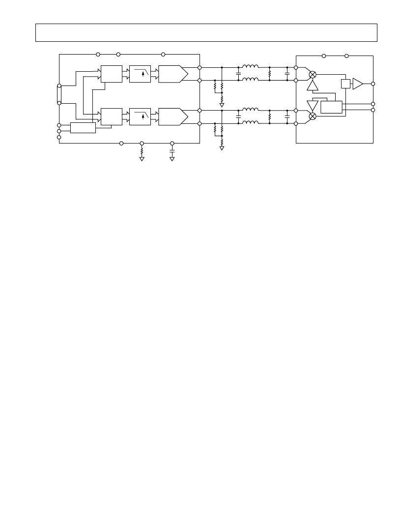
Figure 7. Shows the schematic of the AD8345 evaluation board.
Note that uninstalled components are marked as open. This is a
4-layer board, with the two center layers used as ground plane
and top and bottom layers used as signal and power planes.
The board is powered by a single supply (V
S
) in the range, 2.7 V to
5.5 V. The power supply is decoupled by a 0.01
μ
F and 1000 pF
capacitors. The circuit closely follows the basic connection
schematic with SW1 in B Position. If SW1 is in Position A, the
Enable pin will be pulled to ground by a 10 k
resistor and the
device will be in its power-down mode.
All connectors are SMA-type. The I and Q inputs are dc-coupled
to allow a direct connection to a dual DAC with differential
outputs. Resistor pads are provided in case termination at the
I and Q inputs is required. The local oscillator input (LO) is
terminated to approximately 50
with an external 50
resistor
to ground. A 1:1 wide-band transformer (ETC1-1-13) provides
a differential drive to the AD8345’s differential LO input. The
device can also be driven single-ended by shorting out T1.
33pF
100
310nH
33pF
310nH
51
10
51
33pF
100
310nH
33pF
310nH
51
10
51
PHASE
SPLITTER
VOUT
IBBP
IBBN
QBBP
QBBN
AD8345
LOIP
LOIN
VPS1
VPS2
IOUTB
IOUTA
“
I
”
DAC
2
LATCH
“
I
”
“
Q
”
DAC
2
LATCH
“
Q
”
QOUTA
0.1 F
R
SET
2k
REFIO
FS ADJ
SLEEP
SELECT
WRITE
CLOCK
AD9761
MUX
CONTROL
AVDD
DVDD
DCOM
QOUTB
DAC
DATA
INPUTS
Figure 6. AD8345/TxDAC Interface
相關PDF資料 |
PDF描述 |
|---|---|
| AD8346ARU-REEL | 0.8 GHz-2.5 GHz Quadrature Modulator |
| AD8346 | 0.8 GHz-2.5 GHz Quadrature Modulator |
| AD8346-EVAL | 0.8 GHz-2.5 GHz Quadrature Modulator |
| AD8346ARU | 0.8 GHz-2.5 GHz Quadrature Modulator |
| AD8346ARU-REEL7 | 0.8 GHz-2.5 GHz Quadrature Modulator |
相關代理商/技術參數 |
參數描述 |
|---|---|
| AD8345ARE-REEL | 制造商:Analog Devices 功能描述:Quadrature Mod 80MHz 16-Pin TSSOP EP T/R |
| AD8345ARE-REEL7 | 功能描述:IC QUADRATURE MOD 250MHZ 16TSSOP RoHS:否 類別:RF/IF 和 RFID >> RF 調制器 系列:- 產品培訓模塊:Lead (SnPb) Finish for COTS Obsolescence Mitigation Program 標準包裝:2,500 系列:- 功能:調制器 LO 頻率:700MHz ~ 2.3GHz RF 頻率:700MHz ~ 2.3GHz P1dB:1dBm 底噪:-148dBm/Hz 輸出功率:-1dBm 電流 - 電源:46mA 電源電壓:2.7 V ~ 3.6 V 測試頻率:1.75GHz 封裝/外殼:28-WFQFN 裸露焊盤 包裝:帶卷 (TR) |
| AD8345AREZ | 功能描述:IC QUADRATURE MOD 250MHZ 16TSSOP RoHS:是 類別:RF/IF 和 RFID >> RF 調制器 系列:- 產品培訓模塊:Lead (SnPb) Finish for COTS Obsolescence Mitigation Program 標準包裝:2,500 系列:- 功能:調制器 LO 頻率:700MHz ~ 2.3GHz RF 頻率:700MHz ~ 2.3GHz P1dB:1dBm 底噪:-148dBm/Hz 輸出功率:-1dBm 電流 - 電源:46mA 電源電壓:2.7 V ~ 3.6 V 測試頻率:1.75GHz 封裝/外殼:28-WFQFN 裸露焊盤 包裝:帶卷 (TR) |
| AD8345AREZ | 制造商:Analog Devices 功能描述:IC QUAD MODULATOR 140MHZ-1GHZ 16-TSSO 制造商:Analog Devices 功能描述:IC, QUAD MODULATOR, 140MHZ-1GHZ, 16-TSSO |
| AD8345AREZ-REEL | 制造商:Analog Devices 功能描述:Quadrature Mod 80MHz 16-Pin TSSOP EP T/R |
發布緊急采購,3分鐘左右您將得到回復。