- 您現在的位置:買賣IC網 > PDF目錄373944 > AD8349ARE (ANALOG DEVICES INC) 700 MHz to 2700 MHz Quadrature Modulator PDF資料下載
參數資料
| 型號: | AD8349ARE |
| 廠商: | ANALOG DEVICES INC |
| 元件分類: | 衰減器 |
| 英文描述: | 700 MHz to 2700 MHz Quadrature Modulator |
| 中文描述: | 700 MHz - 2700 MHz RF/MICROWAVE QPSK MODULATOR |
| 封裝: | MO-153ABT, TSSOP-16 |
| 文件頁數: | 14/28頁 |
| 文件大小: | 969K |
| 代理商: | AD8349ARE |
第1頁第2頁第3頁第4頁第5頁第6頁第7頁第8頁第9頁第10頁第11頁第12頁第13頁當前第14頁第15頁第16頁第17頁第18頁第19頁第20頁第21頁第22頁第23頁第24頁第25頁第26頁第27頁第28頁
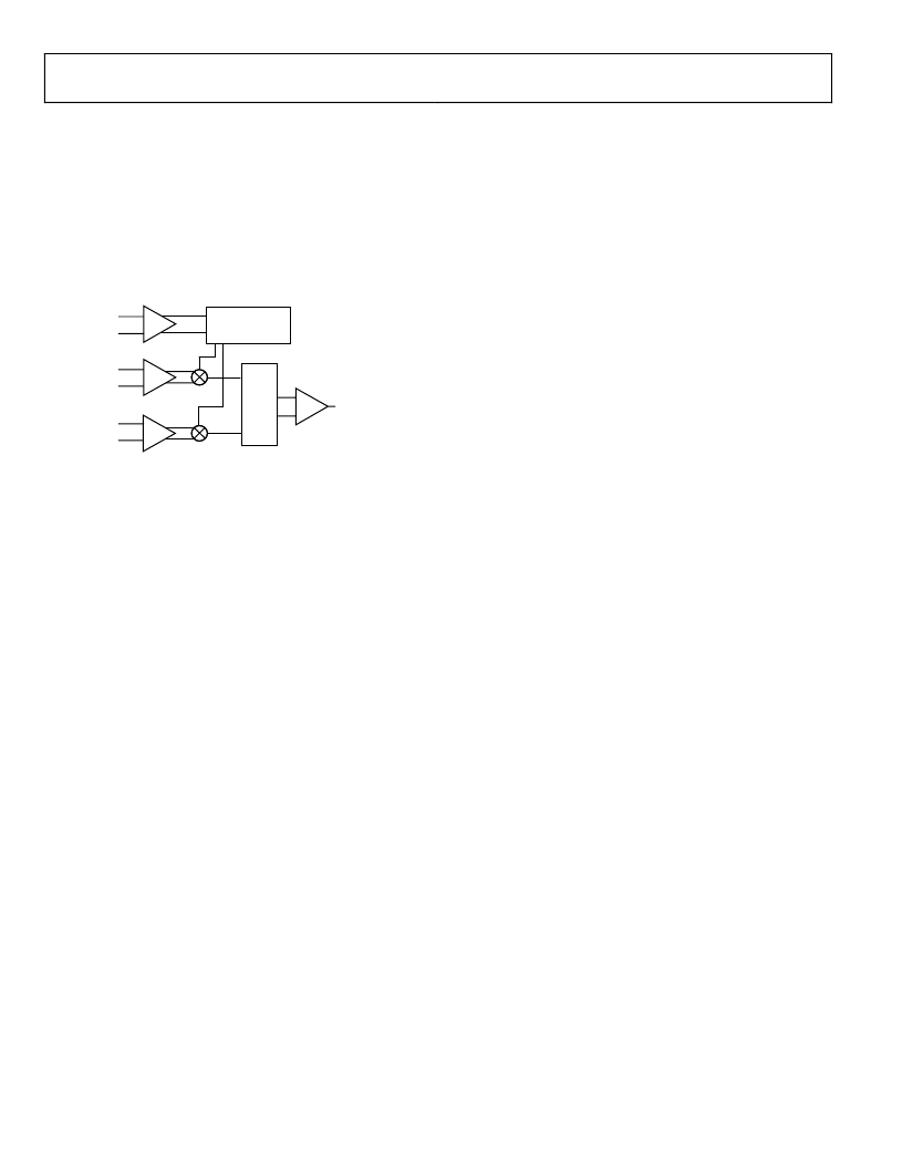
AD8349
CIRCUIT DESCRIPTION
OVERVIEW
The AD8349 can be divided into five sections: the local oscil-
lator (LO) interface, the baseband voltage-to-current (V-to-I)
converter, the mixers, the differential-to-single-ended (D-to-S)
amplifier, and the bias circuit. A detailed block diagram of the
device is shown in Figure 42.
Rev. 0 | Page 14 of 28
PHASE
SPLITTER
OUT
LOIP
LOIN
IBBP
IBBN
QBBP
QBBN
Σ
0
Figure 42. AD8349 Block Diagram
The LO interface generates two LO signals at 90 degrees of
phase difference to drive two mixers in quadrature. Baseband
signals are converted into currents by the V-to-I converters,
which feed into the two mixers. The outputs of the mixers
combine to feed the differential-to-single-ended amplifier,
which provides a 50 output interface. Reference currents to
each section are generated by the bias circuit. Additionally, the
RF output is controlled by an output enable pin (ENOP), which
is capable of switching the output on and off within 50 ns. A
detailed description of each section follows.
LO INTERFACE
The LO interface consists of interleaved stages of buffer
amplifiers and polyphase phase splitters. An input buffer
provides a 50 termination to the LO signal source driving
LOIP and LOIN. The buffer also increases the LO signal
amplitude to drive the phase splitter. The phase splitter is
formed by an R-C polyphase network that splits the buffered
LO signal into two parts in precise quadrature phase relation
with each other. Each LO signal then passes through a buffer
amplifier to compensate for the signal loss through the phase
splitter. The two signals pass through another polyphase
network to enhance the quadrature accuracy over the full
operating frequency range. The outputs of the second phase
splitter are fed into the driver amplifiers for the mixers’ LO
inputs.
V-TO-I CONVERTER
The differential baseband input voltages that are applied to the
baseband input pins are fed to two op amps that perform a
differential voltage-to-current conversion. The differential
output currents of these op amps then feed each of their
respective mixers.
MIXERS
The AD8349 has two double-balanced mixers, one for the in-
phase channel (I channel) and one for the quadrature channel
(Q channel). Both mixers are based on the Gilbert cell design of
four cross-connected transistors. The output currents from the
two mixers sum together in a pair of resistor-inductor (R-L)
loads. The signals developed across the R-L loads are sent to the
D-to-S amplifier.
D-TO-S AMPLIFIER
The output D-to-S amplifier consists of two emitter followers
driving a totem pole output stage. Output impedance is estab-
lished by the emitter resistors in the output transistors. The
output of this stage connects to the output (VOUT) pin.
BIAS CIRCUIT
A band gap reference circuit generates the proportional-to-
absolute-temperature (PTAT) reference currents used by
different sections. The band gap reference circuit also generates
a temperature stable current in the V-to-I converters to produce
a temperature independent slew rate.
OUTPUT ENABLE
During normal operation (ENOP = high), the output current
from the V-to-I converters feeds into the mixers, where they
mix with the two phases of LO signals. When ENOP is pulled
low, the V-to-I output currents are steered away from the
mixers, thus turning off the RF output. Power to the final stage
of LO drivers is also removed to minimize LO feedthrough.
Even when the output is disabled, the differential-to-single-
ended stage is still powered up to maintain constant output
impedance.
相關PDF資料 |
PDF描述 |
|---|---|
| AD8349ARE-REEL7 | 700 MHz to 2700 MHz Quadrature Modulator |
| AD8350 | Low Distortion 1.0 GHz Differential Amplifier |
| AD8350AR15 | Low Distortion 1.0 GHz Differential Amplifier |
| AD8350AR15-EVAL | Low Distortion 1.0 GHz Differential Amplifier |
| AD8350AR15-REEL | Low Distortion 1.0 GHz Differential Amplifier |
相關代理商/技術參數 |
參數描述 |
|---|---|
| AD8349ARE-REEL7 | 功能描述:IC QUADRATURE MOD 700MHZ 16TSSOP RoHS:否 類別:RF/IF 和 RFID >> RF 調制器 系列:- 產品培訓模塊:Lead (SnPb) Finish for COTS Obsolescence Mitigation Program 標準包裝:2,500 系列:- 功能:調制器 LO 頻率:700MHz ~ 2.3GHz RF 頻率:700MHz ~ 2.3GHz P1dB:1dBm 底噪:-148dBm/Hz 輸出功率:-1dBm 電流 - 電源:46mA 電源電壓:2.7 V ~ 3.6 V 測試頻率:1.75GHz 封裝/外殼:28-WFQFN 裸露焊盤 包裝:帶卷 (TR) |
| AD8349AREZ | 功能描述:IC QUADRATURE MOD 700MHZ 16TSSOP RoHS:是 類別:RF/IF 和 RFID >> RF 調制器 系列:- 產品培訓模塊:Lead (SnPb) Finish for COTS Obsolescence Mitigation Program 標準包裝:2,500 系列:- 功能:調制器 LO 頻率:700MHz ~ 2.3GHz RF 頻率:700MHz ~ 2.3GHz P1dB:1dBm 底噪:-148dBm/Hz 輸出功率:-1dBm 電流 - 電源:46mA 電源電壓:2.7 V ~ 3.6 V 測試頻率:1.75GHz 封裝/外殼:28-WFQFN 裸露焊盤 包裝:帶卷 (TR) |
| AD8349AREZ-RL7 | 功能描述:IC MOD QUAD 2.7GHZ 16TSSOP RoHS:是 類別:RF/IF 和 RFID >> RF 調制器 系列:- 產品培訓模塊:Lead (SnPb) Finish for COTS Obsolescence Mitigation Program 標準包裝:2,500 系列:- 功能:調制器 LO 頻率:700MHz ~ 2.3GHz RF 頻率:700MHz ~ 2.3GHz P1dB:1dBm 底噪:-148dBm/Hz 輸出功率:-1dBm 電流 - 電源:46mA 電源電壓:2.7 V ~ 3.6 V 測試頻率:1.75GHz 封裝/外殼:28-WFQFN 裸露焊盤 包裝:帶卷 (TR) |
| AD8349EVAL | 制造商:Analog Devices 功能描述:IC ((NS)) |
| AD8349-EVAL | 制造商:Analog Devices 功能描述:AD8349 EVALUATION BOARD - Bulk |
發布緊急采購,3分鐘左右您將得到回復。