- 您現在的位置:買賣IC網 > PDF目錄373944 > AD8349ARE (ANALOG DEVICES INC) 700 MHz to 2700 MHz Quadrature Modulator PDF資料下載
參數資料
| 型號: | AD8349ARE |
| 廠商: | ANALOG DEVICES INC |
| 元件分類: | 衰減器 |
| 英文描述: | 700 MHz to 2700 MHz Quadrature Modulator |
| 中文描述: | 700 MHz - 2700 MHz RF/MICROWAVE QPSK MODULATOR |
| 封裝: | MO-153ABT, TSSOP-16 |
| 文件頁數: | 19/28頁 |
| 文件大小: | 969K |
| 代理商: | AD8349ARE |
第1頁第2頁第3頁第4頁第5頁第6頁第7頁第8頁第9頁第10頁第11頁第12頁第13頁第14頁第15頁第16頁第17頁第18頁當前第19頁第20頁第21頁第22頁第23頁第24頁第25頁第26頁第27頁第28頁
AD8349
baseband input paths leading to the mixers, perfectly matched
baseband signals at the pins of the device may not be perfectly
matched when they reach the mixers. Therefore, slight
adjustments have to be made to the phase and amplitudes of the
baseband signals to compensate for these mismatches.
Rev. 0 | Page 19 of 28
Begin by making one of the inputs, say the I channel, the
reference signal. Then adjust the amplitude and phase of the Q
channel’s signal until the unwanted sideband power reaches a
trough. The AD9777 has built-in gain adjust registers that allow
this to be performed easily. If an iterative adjustment is
performed between the amplitude and the phase, the undesired
sideband leakage can be minimized significantly.
Note that the compensated sideband rejection performance
degrades as the operating baseband frequency is moved away
from the frequency at which the compensation was performed.
As a result, the frequency of the I and Q sine waves should be
approximately half the baseband bandwidth of the modulated
carrier. For example, if the modulator is being used to transmit
a single WCDMA carrier whose baseband spectrum spans from
dc to 3.84/2 MHz, the calibration could be effectively performed
with 1 MHz I and Q sine waves.
REDUCTION OF LO FEEDTHROUGH
Because the I and Q signals are being multiplied with the LO,
any internal offset voltages on these inputs will result in leakage
of the LO to the output. Additionally, any imbalance in the LO
to RF in the mixers will also cause the LO signal to leak through
the mixer to the RF output. The LO feedthrough is clearly
visible in the single sideband spectrum. The nominal LO
feedthrough of –42 dBm can be reduced further by applying
offset compensation voltages on the I and Q inputs. Note that
the LO feedthrough is reduced by varying the differential offset
voltages on the I and Q inputs (xBBP – xBBN), not by varying
the nominal bias level of 400 mV. This is easily accomplished by
programming and then storing the appropriate DAC offset code
required to minimize the LO feedthrough. This, however,
requires a dc-coupled path from the DAC to the I and Q inputs.
The procedure for reducing the LO feedthrough is simple. A
differential offset voltage is applied from the I DAC until the LO
feedthrough reaches a trough. With this offset level held, a
differential offset voltage is applied to the Q DAC until a lower
trough is reached (This is an iterative process).
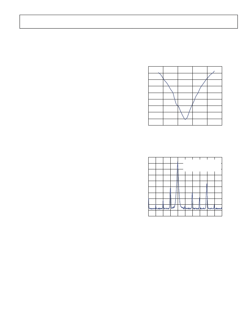
Figure 54 shows a plot of LO feedthrough versus I channel
offset (in mV) after the Q channel offset has been nulled. This
suggests that the compensating offset voltage should have a
resolution of at least 100 μV to reduce the LO feedthrough to be
less than –65 dBm. Figure 55 shows the single sideband
spectrum at 2140 MHz after the nulling of the LO. The reduced
LO feedthrough can clearly be seen when compared with the
performance shown in Figure 53.
Compensated LO feedthrough degrades somewhat as the LO
frequency is moved away from the frequency at which the
compensation was performed. This variation is very small
across a 30 MHz or 60 MHz cellular band, however. This small
variation is due to the effects of LO-to-RF output leakage
around the package and on the board.
–70
–60
–58
–56
–54
–52
C
–62
–68
–66
–64
3.0
4.0
4.5
5.0
5.5
3.5
IOPP-IOPN (mV)
0
Figure 54. Plot of LO Feedthrough vs. I Channel Baseband Offset
(Q Channel Offset Nulled)
–90
–80
–70
–60
–50
–40
–30
–20
–10
0
10
A
CENTER 2.14GHz
SPAN 10MHz
0
SSB = 1.7dBm
LO = –71.4dBm
USB = –52dBc
THIRD HARMONIC = –36.8dBc
Figure 55. AD8349 Single Sideband Spectrum at 2140 MHz after LO Nulling
SIDEBAND SUPPRESSION AND LO FEEDTHROUGH
VERSUS TEMPERATURE
In practical applications, reduction of LO feedthrough and
undesired sideband suppression can be performed as a one time
calibration, with the required correction factors being stored in
nonvolatile RAM. These compensation schemes hold up well
over temperature. Figure 40 and Figure 41 show the variation in
LO feedthrough and sideband suppression over temperature
after compensation is performed at 25°C.
相關PDF資料 |
PDF描述 |
|---|---|
| AD8349ARE-REEL7 | 700 MHz to 2700 MHz Quadrature Modulator |
| AD8350 | Low Distortion 1.0 GHz Differential Amplifier |
| AD8350AR15 | Low Distortion 1.0 GHz Differential Amplifier |
| AD8350AR15-EVAL | Low Distortion 1.0 GHz Differential Amplifier |
| AD8350AR15-REEL | Low Distortion 1.0 GHz Differential Amplifier |
相關代理商/技術參數 |
參數描述 |
|---|---|
| AD8349ARE-REEL7 | 功能描述:IC QUADRATURE MOD 700MHZ 16TSSOP RoHS:否 類別:RF/IF 和 RFID >> RF 調制器 系列:- 產品培訓模塊:Lead (SnPb) Finish for COTS Obsolescence Mitigation Program 標準包裝:2,500 系列:- 功能:調制器 LO 頻率:700MHz ~ 2.3GHz RF 頻率:700MHz ~ 2.3GHz P1dB:1dBm 底噪:-148dBm/Hz 輸出功率:-1dBm 電流 - 電源:46mA 電源電壓:2.7 V ~ 3.6 V 測試頻率:1.75GHz 封裝/外殼:28-WFQFN 裸露焊盤 包裝:帶卷 (TR) |
| AD8349AREZ | 功能描述:IC QUADRATURE MOD 700MHZ 16TSSOP RoHS:是 類別:RF/IF 和 RFID >> RF 調制器 系列:- 產品培訓模塊:Lead (SnPb) Finish for COTS Obsolescence Mitigation Program 標準包裝:2,500 系列:- 功能:調制器 LO 頻率:700MHz ~ 2.3GHz RF 頻率:700MHz ~ 2.3GHz P1dB:1dBm 底噪:-148dBm/Hz 輸出功率:-1dBm 電流 - 電源:46mA 電源電壓:2.7 V ~ 3.6 V 測試頻率:1.75GHz 封裝/外殼:28-WFQFN 裸露焊盤 包裝:帶卷 (TR) |
| AD8349AREZ-RL7 | 功能描述:IC MOD QUAD 2.7GHZ 16TSSOP RoHS:是 類別:RF/IF 和 RFID >> RF 調制器 系列:- 產品培訓模塊:Lead (SnPb) Finish for COTS Obsolescence Mitigation Program 標準包裝:2,500 系列:- 功能:調制器 LO 頻率:700MHz ~ 2.3GHz RF 頻率:700MHz ~ 2.3GHz P1dB:1dBm 底噪:-148dBm/Hz 輸出功率:-1dBm 電流 - 電源:46mA 電源電壓:2.7 V ~ 3.6 V 測試頻率:1.75GHz 封裝/外殼:28-WFQFN 裸露焊盤 包裝:帶卷 (TR) |
| AD8349EVAL | 制造商:Analog Devices 功能描述:IC ((NS)) |
| AD8349-EVAL | 制造商:Analog Devices 功能描述:AD8349 EVALUATION BOARD - Bulk |
發布緊急采購,3分鐘左右您將得到回復。