- 您現在的位置:買賣IC網 > PDF目錄373945 > AD835 (Analog Devices, Inc.) 250 MHz, Voltage Output 4-Quadrant Multiplier PDF資料下載
參數資料
| 型號: | AD835 |
| 廠商: | Analog Devices, Inc. |
| 英文描述: | 250 MHz, Voltage Output 4-Quadrant Multiplier |
| 中文描述: | 250,電壓輸出4兆赫的象限乘法器 |
| 文件頁數: | 6/8頁 |
| 文件大小: | 200K |
| 代理商: | AD835 |
AD835
REV. A
–6–
Simplified representations of this sort, where all signals are pre-
sumed to be expressed in
volts
, are used throughout this data
sheet, to avoid the needless use of less-intuitive subscripted vari-
ables (such as V
). We can view all variables as being
normal-
ized to 1 V
. For example, the input X can either be stated as
being in the range –1 V to +1 V, or simply –1 to +1. T he latter
representation will be found to facilitate the development of new
functions using the AD835. T he explicit inclusion of the de-
nominator, U, is also less helpful, as in the case of the AD835, if
it is not an electrical input variable.
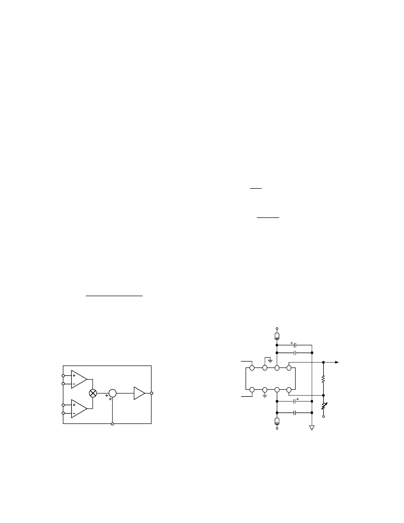
Scaling Adjustment
T he basic value of U in Equation 1 is nominally 1.05 V. Figure
18, which shows the basic multiplier connections, also
shows how the effective value of U can be adjusted to have any
lower voltage (usually 1 V) through the use of a resistive-divider
between W (Pin 5) and Z (Pin 4). Using the general resistor val-
ues shown, we can rewrite Equation 1 as
W
=
X Y
U
+
kW
+
(1±
k
)
Z
(3)
(where Z' is distinguished from the signal Z at Pin 4). It follows
that
(4)
In this way, we can modify the effective value of U to
U
=
(1±
k
)
U
(5)
without altering the scaling of the Z' input. (T his is to be ex-
pected, since the only “ground reference” for the output is
through the Z' input.)
T hus, to set U' to 1 V, remembering that the basic value of U is
1.05 V, we need to choose R1 to have a nominal value of 20
times R2. T he values shown here allow U to be adjusted
through the nominal range 0.95 V to 1.05 V, that is, R2 pro-
vides a 5% gain adjustment.
Figure 18. Multiplier Connections
Note that in many applications, the exact gain of the multiplier
may not be very important; in which case, this network may be
omitted entirely, or R2 fixed at 100
.
PRODUCT DE SCRIPT ION
T he AD835 is a four-quadrant, voltage output, analog multi-
plier fabricated on an advanced, dielectrically isolated, comple-
mentary bipolar process. In its basic mode, it provides the linear
product of its X and Y voltage inputs. In this mode, the –3dB
output voltage bandwidth is 250 MHz (a small signal rise time
of 1 ns). Full-scale (–1 V to +1 V) rise/fall times are 2.5 ns (with
the standard R
of 150
) and the settling time to 0.1% under
the same conditions is typically 20 ns.
As in earlier multipliers from Analog Devices, a unique sum-
ming feature is provided at the Z-input. As well as providing in-
dependent ground references for inputs and output, and
enhanced versatility, this feature allows the AD835 to operate
with voltage
gain
. Its X -, Y- and Z-input voltages are all nomi-
nally
±
1 V FS, with overrange of at least 20%. T he inputs are
fully differential and at high impedance (100 k
i
2 pF) and pro-
vide a 70 dB CMRR (f
≤
1 MHz).
T he low impedance output is capable of driving loads as small
as 25
. T he peak output can be as large as
±
2.2 V minimum
for R
= 150
, or
±
2.0 V minimum into R
= 50
. T he
AD835 has much lower noise than the AD534 or AD734, mak-
ing it attractive in low level signal-processing applications, for
example, as a wideband gain-control element or modulator.
Basic T heory
T he multiplier is based on a classic form, having a translinear
core, supported by three (X , Y, Z) linearized voltage-to-current
converters, and the load driving output amplifier. T he scaling
voltage (the denominator U, in the equations below) is provided
by a bandgap reference of novel design, optimized for ultralow
noise. Figure 17 shows the functional block diagram.
In general terms, the AD835 provides the function
W
=
(
X
1±
X
2)(
Y
1±
Y
2)
U
+
Z
(1)
where the variables W, U, X , Y and Z are all voltages. Con-
nected as a simple multiplier, with X = X 1 – X 2, Y = Y1 – Y2
and Z = 0, and with a scale factor adjustment (see below) which
sets U = 1 V, the output can be expressed as
W = X Y
(2)
Figure 17. Functional Block Diagram
Y1
Y2
Z INPUT
Y = Y1
–Y2
X = X1
–X2
XY + Z
X1
X2
W OUTPUT
XY
AD835
∑
+1
X Y
R1 = (1–k) R
2k
W
R2 = kR
+5V
X1
X2
AD835
VP
W
Z
4
VN
3
Y2
2
Y1
1
X1
FB
+5V
X
Y
–5V
Z
1
FB
5
7
0.01
μ
F CERAMIC
4.7
μ
F TANTALUM
8
0.01
μ
F CERAMIC
4.7
μ
F TANTALUM
6
相關PDF資料 |
PDF描述 |
|---|---|
| AD835AN | 250 MHz, Voltage Output 4-Quadrant Multiplier |
| AD835AR | 250 MHz, Voltage Output 4-Quadrant Multiplier |
| ad8360 | DC-2.5GHz TruePower Detector/Controller(RMS-DC轉換器) |
| AD8361 | LF to 2.5 GHz TruPwr⑩ Detector |
| AD8361ARM | LF to 2.5 GHz TruPwr⑩ Detector |
相關代理商/技術參數 |
參數描述 |
|---|---|
| AD8350 | 制造商:AD 制造商全稱:Analog Devices 功能描述:Low Distortion 1.0 GHz Differential Amplifier |
| AD8350_01 | 制造商:AD 制造商全稱:Analog Devices 功能描述:Low Distortion 1.0 GHz Differential Amplifier |
| AD8350AR15 | 制造商:Analog Devices 功能描述:SP Amp DIFF AMP Single 11V 8-Pin SOIC N Tube 制造商:Rochester Electronics LLC 功能描述:SOIC G=15DB LO DISTORT'N 1.2GHZ DIFF AMP - Bulk 制造商:Analog Devices 功能描述:IC AMP DIFFERENTIAL |
| AD8350AR15-EVAL | 制造商:Analog Devices 功能描述:Evaluation Board For AD8350 Differential Amplifier 制造商:Analog Devices 功能描述:EVAL BD FOR AD8350 DIFFERENTIAL AMP - Bulk |
| AD8350AR15-REEL | 制造商:Analog Devices 功能描述:SP Amp DIFF AMP Single 11V 8-Pin SOIC N T/R 制造商:Analog Devices 功能描述:SP AMP DIFF AMP SGL 11V 8SOIC N - Tape and Reel 制造商:Rochester Electronics LLC 功能描述:SOIC G=15DB LO DISTORT'N 1.2GHZ DIFF AMP - Tape and Reel |
發布緊急采購,3分鐘左右您將得到回復。