- 您現(xiàn)在的位置:買賣IC網(wǎng) > PDF目錄373945 > AD8361ART-REEL7 (ANALOG DEVICES INC) LF to 2.5 GHz TruPwr⑩ Detector PDF資料下載
參數(shù)資料
| 型號: | AD8361ART-REEL7 |
| 廠商: | ANALOG DEVICES INC |
| 元件分類: | 模擬信號調(diào)理 |
| 英文描述: | LF to 2.5 GHz TruPwr⑩ Detector |
| 中文描述: | SPECIALTY ANALOG CIRCUIT, PDSO6 |
| 封裝: | MO-178-AB, SOT-23, 6 PIN |
| 文件頁數(shù): | 11/16頁 |
| 文件大小: | 306K |
| 代理商: | AD8361ART-REEL7 |
AD8361
–11–
REV. A
INPUT
–
mV
700
200
0
500
100
200
300
400
500
400
300
600
m
100
0
600
700
800
Figure 37. Idealized Output Step Size as Function of Input
Voltage
Plots of output voltage vs. input voltage result in a straight line. It
may sometimes be more useful to plot the error on a logarith-
mic scale, as shown in Figure 38. The deviation of the plot for
the ideal straight line characteristic is caused by output clipping
at the high end and by signal offsets at the low end. It should
however be noted that offsets at the low end can be either posi-
tive or negative, so that this plot could also trend upwards at the
low end. Figures 5, 6, 8, and 9 show a
±
3 sigma distribution of
device error for a large population of devices.
INPUT
–
V rms
2.0
–
0.5
0.01
0.5
0.0
1.5
1.0
E
–
–
1.0
–
1.5
–
2.0
1.0
1.9GHz
2.5GHz
900MHz
100MHz
100MHz
0.02
(
–
21dBm)
0.1
(
–
7dBm)
0.4
(+5dBm)
Figure 38. Representative Unit, Error in dB vs. Input Level,
V
S
= 2.7 V
It is also apparent in Figure 38 that the error plot tends to
shift to the right with increasing frequency. Because the input
impedance decreases with frequency, the voltage actually applied
to the input will also tend to decrease (assuming a constant source
impedance over frequency). The dynamic range is almost con-
stant over frequency, but with a small decrease in conversion gain
at high frequency.
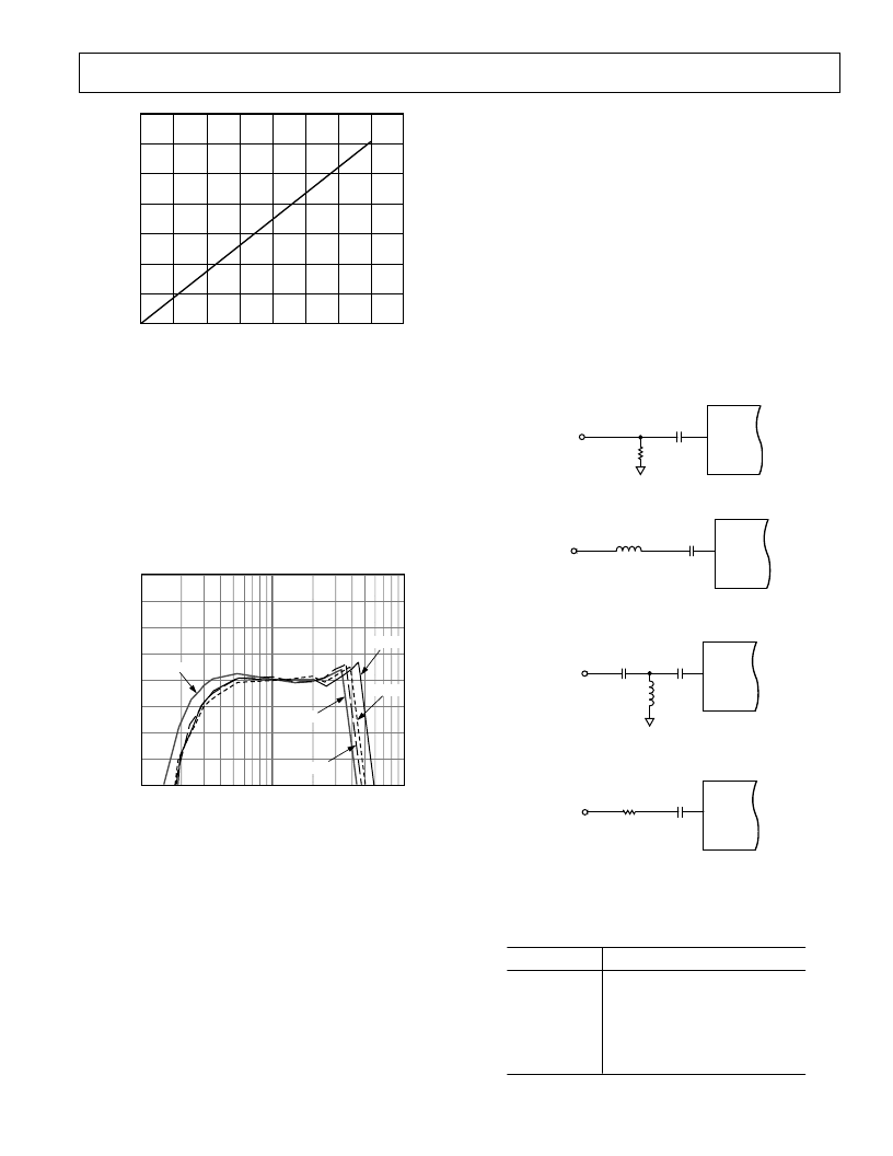
Input Coupling and Matching
The input impedance of the AD8361 decreases with increasing
frequency in both its resistive and capacitive components (Figure
13). The resistive component varies from 225
at 100 MHz
down to about 95
at 2.5 GHz.
A number of options exist for input matching. For operation at
multiple frequencies, a 75
shunt to ground, as shown in Figure
39a, will provide the best overall match. For use at a single fre-
quency, a resistive or a reactive match can be used. By plotting the
input impedance on a Smith Chart, the best value for a
resistive match can be calculated. The VSWR can be held below
1.5 at frequencies up to 1 GHz, even as the input impedance
varies from part to part. (Both input impedance and input
capacitance can vary by up to
±
20% around their nominal values.)
At very high frequencies (i.e., 1.8 GHz to 2.5 GHz), a shunt
resistor will not be suf
fi
cient to reduce the VSWR below 1.5.
Where VSWR is critical, remove shunt component and insert
an inductor in series with the coupling capacitor as shown in
Figure 39b.
Table II gives recommended shunt resistor values for various
frequencies and series inductor values for high frequencies. The
coupling capacitor, C
C
, essentially acts as an ac-short and plays
no intentional part in the matching.
AD8361
RFIN
RFIN
R
SH
C
C
a. Broadband Resistor Match
AD8361
C
C
RFIN
RFIN
L
M
b. Series Inductor Match
AD8361
C
C
RFIN
RFIN
L
M
C
M
c. Narrowband Reactive Match
AD8361
C
C
RFIN
RFIN
R
SERIES
d. Attenuating the Input Signal
Figure 39. Input Coupling/Matching Options
Table II. Recommended Component Values for Resistive or
Inductive Input Matching (Figures 39a and 39b)
Frequency
Matching Component
63.4
Shunt
75
Shunt
75
Shunt
150
Shunt or 4.7 nH Series
150
Shunt or 4.7 nH Series
150
Shunt or 2.7 nH Series
100 MHz
800 MHz
900 MHz
1800 MHz
1900 MHz
2500 MHz
相關(guān)PDF資料 |
PDF描述 |
|---|---|
| AD8361-EVAL | LF to 2.5 GHz TruPwr⑩ Detector |
| AD8362 | 50 Hz to 2.7 GHz 60 dB TruPwr⑩ Detector |
| AD8362-EVAL | 50 Hz to 2.7 GHz 60 dB TruPwr⑩ Detector |
| AD8362ARU | 50 Hz to 2.7 GHz 60 dB TruPwr⑩ Detector |
| AD8362ARU-REEL7 | 50 Hz to 2.7 GHz 60 dB TruPwr⑩ Detector |
相關(guān)代理商/技術(shù)參數(shù) |
參數(shù)描述 |
|---|---|
| AD8361ARTZ | 制造商:Analog Devices 功能描述:IC PWR DETECTOR 2.5GHZ 6SOT23 制造商:Analog Devices 功能描述:IC, PWR DETECTOR, 2.5GHZ, 6SOT23 制造商:Analog Devices 功能描述:IC, PWR DETECTOR, 2.5GHZ, 6SOT23, Frequency Min:100MHz, Frequency Max:2.5GHz, RF Type:CDMA, W-CDMA, QAM, Sensitivity:-, RF IC Case Style:SOT-23, No. of Pins:6, Supply Voltage Min:2.7V, Supply Voltage Max:5.5V, Supply Current:1.1mA, , RoHS Compliant: Yes 制造商:Analog Devices 功能描述:LF TO 2.5 GHZ TRUPWR DETECTOR |
| AD8361ARTZ-RL | 制造商:Analog Devices 功能描述: |
| AD8361ARTZ-RL7 | 功能描述:IC PWR DETECTOR 2.5GHZ SOT23-6 RoHS:是 類別:RF/IF 和 RFID >> RF 檢測器 系列:- 產(chǎn)品變化通告:Product Discontinuation 15/May/2006 標(biāo)準(zhǔn)包裝:3,000 系列:- 頻率:100MHz ~ 2GHz RF 型:手機(jī),GSM,DCS,PCS 輸入范圍:- 精確度:- 電源電壓:2.7 V ~ 5.5 V 電流 - 電源:300µA 包裝:帶卷 (TR) 封裝/外殼:SC-74,SOT-457 其它名稱:NCS5000SNT1GOS |
| AD8361ARTZ-RL7 | 制造商:Analog Devices 功能描述:RMS DETECTOR IC ((NW)) |
| AD8361-EVAL | 制造商:Analog Devices 功能描述:AD8361 EVALUATION BOARD - Bulk |
發(fā)布緊急采購,3分鐘左右您將得到回復(fù)。