- 您現在的位置:買賣IC網 > PDF目錄373945 > AD8362-EVAL (Analog Devices, Inc.) 50 Hz to 2.7 GHz 60 dB TruPwr⑩ Detector PDF資料下載
參數資料
| 型號: | AD8362-EVAL |
| 廠商: | Analog Devices, Inc. |
| 英文描述: | 50 Hz to 2.7 GHz 60 dB TruPwr⑩ Detector |
| 中文描述: | 50赫茲到2.7 GHz 60分貝TruPwr⑩探測器 |
| 文件頁數: | 27/36頁 |
| 文件大小: | 700K |
| 代理商: | AD8362-EVAL |
第1頁第2頁第3頁第4頁第5頁第6頁第7頁第8頁第9頁第10頁第11頁第12頁第13頁第14頁第15頁第16頁第17頁第18頁第19頁第20頁第21頁第22頁第23頁第24頁第25頁第26頁當前第27頁第28頁第29頁第30頁第31頁第32頁第33頁第34頁第35頁第36頁
AD8362
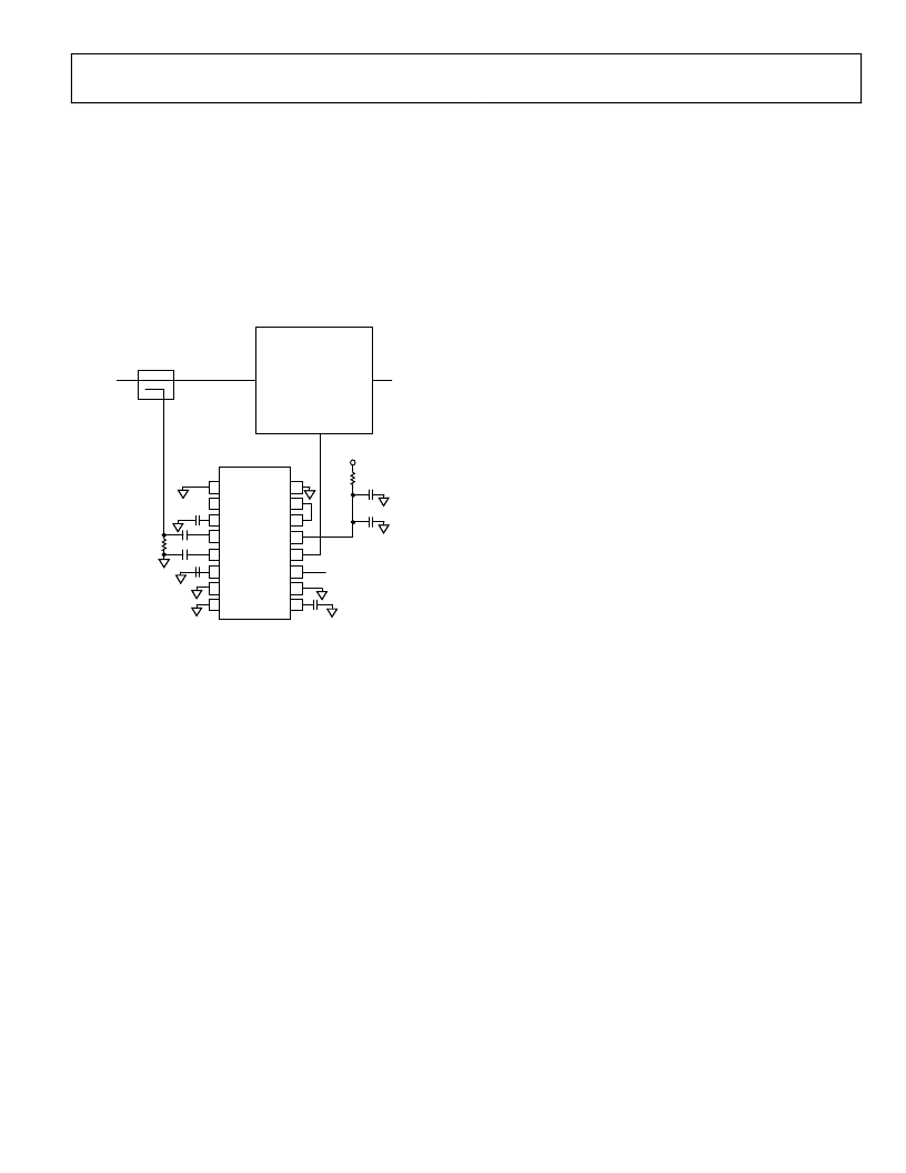
OPERATOR IN CONTROLLER MODES
In order to fully understand this section, it is important to first
read the preceding discussion of measurement modes, because
there are only a few differences in operation and connections.
When used in controller applications, the basic objective is to
use the AD8362 as a level-sensing element in such a way that its
output, here V
APC
, moves in a direction that increases the
controlled signal when the input sample is too low, and vice
versa. A general scheme is shown in Figure 60.
Rev. B | Page 27 of 36
V
S
SETPOINT
VOLTAGE INPUT
0.5V TO 3.5V
CONTROLLED SYSTEM
(OUTPUT POWER
DECREASES AS V
APC
INCREASES)
OUTPUT
INPUT
V
APC
SYSTEM
INPUT
SYSTEM
OUTPUT
C
LPF
1nF
1nF
1nF
R
= 100
FOR 50
TERMINATION
NC
0.1
μ
F
1nF
1nF
3.3
R
SH
16
15
14
13
12
11
10
9
1
2
3
4
5
6
7
8
COMM
CHPF
DECL
INHI
INLO
DECL
PWDN
COMM
ACOM
VREF
VTGT
VPOS
VOUT
VSET
ACOM
CLPF
AD8362
0
Figure 60. Generalized Control Loop Using the AD8362
Because the AD8362 integrates any input error relative to the
setpoint, and ideally would fully null this error over an
appropriate time interval, it follows that V
APC
swings rail-
to-rail over a very narrow range of inputs. In practice, a few
millidecibels of amplitude deviation at the input fully swing the
output.
The signal input level at which this occurs (the setpoint) is
determined by the control voltage, VSET. This voltage defines
the narrow range of the ac input over which the AD8362’s
output is most sensitive to the absolute input magnitude. In base
stations, for example, VSET is often delivered by the ramp DAC,
and the setpoint is a rapidly varying sequence of levels during
the ramp-up and ramp-down intervals of each burst as well as
with output power demand variations from one channel to
another.
Every value of VSET maps uniquely to a specific rms value at its
input. Thus, the major loop shown in Figure 60 forces the
system being controlled to deliver exactly this level (which may
be either in voltage form or as a sample of the power output).
This mode of operation is therefore just an extension of the
measurement mode, having exactly the same scaling (slope and
intercept) at the VSET pin.
When the system in Figure 60 is an RF power amplifier (PA), a
practical consideration immediately comes to our attention.
Frequently, the gain (and thus output power) is arranged to
increase in response to an increasing positive voltage applied to
the gain control pin. However, the AD8362’s output tends
toward higher values as its input crosses over the level
corresponding to the setpoint, which would cause the PA’s
output to increase further. In other words, the feedback polarity
is reversed, forcing the control loop to latch up at one of its
power extremes.
An increasing number of modular PAs feature a control polarity
that reduces the power output with increases in control voltage.
These can be controlled directly from the VOUT pin of the
AD8362. Elsewhere, it is necessary to provide the sign inversion
using a low noise buffer. This amplifier may also include
provisions to ensure that the PA is never driven beyond its safe
limits. The complete details of such a control system depends
on many factors, and this example shows only generic aspects of
the design.
USE OF AN INPUT BALUN
A balun (balance to unbalance) is used either to transform
differential RF signals to single-ended form or in reverse to
convert single-sided signals to differential form. A typical balun
consists of a short length of transmission line (miniature coaxial
or twisted pair) through which the signal passes without
significant degradation, wound on a core (often a ferrite) to
generate a series mode inductor having a high reactive
impedance, compared to the through-mode impedance of the
transmission line, which is often 50 .
High frequency common-mode voltages applied to the input of
this line are sustained across this series reactance and do not
appear at the loaded side of the line. On the other hand, the
through-mode bandwidth is very high, and the losses incurred
in a short line of this sort are trivial.
Baluns of slightly more elaborate construction can provide an
impedance transformation (usually designated by their
impedance ratio, for example, 4:1, which becomes a 1:4 ratio
when used in reverse) in order to convert a single-sided signal
to the balanced form, as is desirable in driving the AD8362,
while also presenting a 50 input interface.
相關PDF資料 |
PDF描述 |
|---|---|
| AD8362ARU | 50 Hz to 2.7 GHz 60 dB TruPwr⑩ Detector |
| AD8362ARU-REEL7 | 50 Hz to 2.7 GHz 60 dB TruPwr⑩ Detector |
| AD8362ARUZ-REEL71 | 50 Hz to 2.7 GHz 60 dB TruPwr⑩ Detector |
| AD8362ARUZ1 | 50 Hz to 2.7 GHz 60 dB TruPwr⑩ Detector |
| AD8367ARU-REEL | 500 MHz, Linear-in-dB VGA with AGC Detector |
相關代理商/技術參數 |
參數描述 |
|---|---|
| AD8362-EVALZ | 功能描述:BOARD EVAL FOR AD8362 RoHS:是 類別:RF/IF 和 RFID >> RF 評估和開發套件,板 系列:TruePower™ 標準包裝:1 系列:- 類型:GPS 接收器 頻率:1575MHz 適用于相關產品:- 已供物品:模塊 其它名稱:SER3796 |
| AD8363 | 制造商:AD 制造商全稱:Analog Devices 功能描述:50 Hz to 6 GHz, 50 dB TruPwr? Detector |
| AD8363_09 | 制造商:AD 制造商全稱:Analog Devices 功能描述:50 Hz to 6 GHz, 50 dB TruPwr? Detector |
| AD8363ACPZ-R2 | 制造商:Analog Devices 功能描述:TRUE RMS PWR DETECTOR 24LFCSP EP - Tape and Reel |
| AD8363ACPZ-R7 | 功能描述:IC DETECTOR RF/IF TRUPWR 16LFCSP RoHS:是 類別:RF/IF 和 RFID >> RF 檢測器 系列:- 產品變化通告:Product Discontinuation 15/May/2006 標準包裝:3,000 系列:- 頻率:100MHz ~ 2GHz RF 型:手機,GSM,DCS,PCS 輸入范圍:- 精確度:- 電源電壓:2.7 V ~ 5.5 V 電流 - 電源:300µA 包裝:帶卷 (TR) 封裝/外殼:SC-74,SOT-457 其它名稱:NCS5000SNT1GOS |
發布緊急采購,3分鐘左右您將得到回復。