- 您現(xiàn)在的位置:買賣IC網(wǎng) > PDF目錄373945 > AD8362ARUZ1 (Analog Devices, Inc.) 50 Hz to 2.7 GHz 60 dB TruPwr⑩ Detector PDF資料下載
參數(shù)資料
| 型號(hào): | AD8362ARUZ1 |
| 廠商: | Analog Devices, Inc. |
| 英文描述: | 50 Hz to 2.7 GHz 60 dB TruPwr⑩ Detector |
| 中文描述: | 50赫茲到2.7 GHz 60分貝TruPwr⑩探測器 |
| 文件頁數(shù): | 23/36頁 |
| 文件大小: | 700K |
| 代理商: | AD8362ARUZ1 |
第1頁第2頁第3頁第4頁第5頁第6頁第7頁第8頁第9頁第10頁第11頁第12頁第13頁第14頁第15頁第16頁第17頁第18頁第19頁第20頁第21頁第22頁當(dāng)前第23頁第24頁第25頁第26頁第27頁第28頁第29頁第30頁第31頁第32頁第33頁第34頁第35頁第36頁
AD8362
An approximate schematic of the signal input section of the
AD8362 is shown in Figure 52. The ladder attenuator is
composed of 11 sections (12 taps), each of which progressively
attenuates the input signal by 6.33 dB. Each tap is connected to
a variable transconductance cell whose bias current determines
the signal weighting given to that tap. The interpolator
determines which stages are active by generating a discrete set
of bias currents, each having a Gaussian profile. These are
arranged to move from left to right, thereby determining the
attenuation applied to the input signal as the gain is
progressively lowered over the 69.3 dB range under control of
the VSET input. The detailed manner in which the
transconductance of adjacent stages varies as the virtual tap
point slides along the attenuator accounts for the ripple
observed in the conformance curves. Its magnitude is slightly
temperature dependent and also varies with frequency (see
Figure 10 to Figure 12). Notice that the system’s responses to
signal inputs at INHI and INLO are not completely
independent; these pins do not constitute a fully floating
differential input.
Rev. B | Page 23 of 36
TO FIXED
GAIN STAGE
gm
gm
gm
gm
ATTENUATION
CONTROL
GUASSIAN INTERPOLATOR
STAGE 1
6.33dB
STAGE 11
6.33dB
INHI
STAGE 2
6.33dB
DECL
INLO
0
Figure 52. Simplified Input Circuit
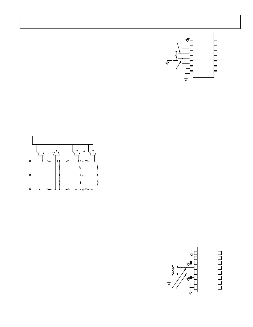
ALTERNATIVE INPUT COUPLING MEANS
The input stages of the AD8362 are optimally driven from a
fully balanced source, which should be provided wherever
possible. The ac low sides of both halves of the attenuator
internally connect to the DECL pin, which is therefore the RF
signal low terminal for both INHI and INLO. In many cases,
unbalanced sources can be applied directly to one or the other
of these two pins. The chief disadvantage of this driving method
is a reduction in dynamic range, particularly at very high
frequencies.
16
15
14
13
12
11
10
9
1
2
3
4
5
6
7
8
COMM
CHPF
DECL
INHI
INLO
DECL
PWDN
COMM
ACOM
VREF
VTGT
VPOS
VOUT
VSET
ACOM
CLPF
AD8362
RF INPUT
Z = 50
NC
THIS INPUT
IS DRIVEN
1nF
1nF
R
SH
DECL AND
INLO ARE
NOT DRIVEN
0
Figure 53. Input Coupling from a Single-Ended Source
Figure 53 illustrates one of many ways of coupling the signal
source to the AD8362. Because the input pins are biased to
about 3.6 V (for V
S
= 5 V) dc-blocking capacitors are required
when driving from a grounded source. For signal frequencies
>5 MHz, a value of 1 nF is adequate. While either INHI or
INLO may be used, INHI is chosen here, and INLO is
connected to the low side of the source. The resistor R
SH
is not
needed if a 100 termination is acceptable. The corresponding
intercept is still 67 dBV, that is, 447 μV rms. However, specified
in power terms at 100 , the P
Z
is now at 2 nW or 57 dBm.
For a source termination of 50 , the internal 100 from INHI
to DECL must be shunted by a chip resistor of 100 . At high
frequencies, a low attenuation pad at the input improves the
VSWR. For example, with a resistor of R
SH
= 33 and an added
resistor of 25 from the source to INHI, a termination of 50
is provided, with 6 dB of attenuation, raising the intercept to
48 dBm.
USING A NARROW-BAND INPUT MATCH
While transformers offer the simplest method for providing
single-sided to balanced conversion, a good alternative is
using a specially designed narrow-band LC network, shown in
Figure 54, which also provides an input match. Using this basic
formulation, the match is to 50 , with a voltage gain of 1.5
(3.56 dB) from the input connector to the AD8362. This
network is specially designed to provide a high degree of
amplitude balance at INHI and INLO as well as an exact phase
inversion. The narrow-band match provides a useful degree of
frequency selectivity, and the capacitors also serve to provide
the required dc blocking.
16
15
14
13
12
11
10
9
1
2
3
4
5
6
7
8
COMM
CHPF
DECL
INHI
INLO
DECL
PWDN
COMM
ACOM
VREF
VTGT
VPOS
VOUT
VSET
ACOM
CLPF
AD8362
RF INPUT
Z = 50
L
NC
THESE INPUTS ARE
EQUAL IN AMPLITUDE
AND OF OPPOSITE SIGN
C2
C1
100
0
Figure 54. Narrow-Band Reactive Input Coupling
相關(guān)PDF資料 |
PDF描述 |
|---|---|
| AD8367ARU-REEL | 500 MHz, Linear-in-dB VGA with AGC Detector |
| AD8367-EVAL | RECTIFIER STANDARD SINGLE 1A 50V 50 30A-ifsm 5uA-ir 1V-vf DO-41 5K/REEL-13 |
| AD8367ARU-REEL-7 | 500 MHz, Linear-in-dB VGA with AGC Detector |
| AD8367 | 500 MHz, Linear-in-dB VGA with AGC Detector |
| AD8367ARU | 500 MHz, Linear-in-dB VGA with AGC Detector |
相關(guān)代理商/技術(shù)參數(shù) |
參數(shù)描述 |
|---|---|
| AD8362ARUZ-REEL7 | 功能描述:IC PWR DETECTOR 3.8GHZ 16-TSSOP RoHS:是 類別:RF/IF 和 RFID >> RF 檢測器 系列:- 產(chǎn)品變化通告:Product Discontinuation 15/May/2006 標(biāo)準(zhǔn)包裝:3,000 系列:- 頻率:100MHz ~ 2GHz RF 型:手機(jī),GSM,DCS,PCS 輸入范圍:- 精確度:- 電源電壓:2.7 V ~ 5.5 V 電流 - 電源:300µA 包裝:帶卷 (TR) 封裝/外殼:SC-74,SOT-457 其它名稱:NCS5000SNT1GOS |
| AD8362ARUZ-REEL71 | 制造商:AD 制造商全稱:Analog Devices 功能描述:50 Hz to 2.7 GHz 60 dB TruPwr⑩ Detector |
| AD8362-EVAL | 制造商:Analog Devices 功能描述:RF DETECTOR, 50 HZ TO 2.7GHZ 60 DB TRUPWR DETECTOR - Bulk |
| AD8362-EVALZ | 功能描述:BOARD EVAL FOR AD8362 RoHS:是 類別:RF/IF 和 RFID >> RF 評(píng)估和開發(fā)套件,板 系列:TruePower™ 標(biāo)準(zhǔn)包裝:1 系列:- 類型:GPS 接收器 頻率:1575MHz 適用于相關(guān)產(chǎn)品:- 已供物品:模塊 其它名稱:SER3796 |
| AD8363 | 制造商:AD 制造商全稱:Analog Devices 功能描述:50 Hz to 6 GHz, 50 dB TruPwr? Detector |
發(fā)布緊急采購,3分鐘左右您將得到回復(fù)。