- 您現在的位置:買賣IC網 > PDF目錄373945 > AD8370ARE (ANALOG DEVICES INC) LF to 750 MHz Digitally Controlled VGA PDF資料下載
參數資料
| 型號: | AD8370ARE |
| 廠商: | ANALOG DEVICES INC |
| 元件分類: | 模擬信號調理 |
| 英文描述: | LF to 750 MHz Digitally Controlled VGA |
| 中文描述: | SPECIALTY ANALOG CIRCUIT, PDSO16 |
| 封裝: | MO-153ABT, TSSOP-16 |
| 文件頁數: | 16/28頁 |
| 文件大小: | 1043K |
| 代理商: | AD8370ARE |
第1頁第2頁第3頁第4頁第5頁第6頁第7頁第8頁第9頁第10頁第11頁第12頁第13頁第14頁第15頁當前第16頁第17頁第18頁第19頁第20頁第21頁第22頁第23頁第24頁第25頁第26頁第27頁第28頁
AD8370
Rev. 0 | Page 16 of 28
The high gain range has better linearity and SFDR at
higher gains.
Conversely, the low gain range has higher SFDR at lower
gains.
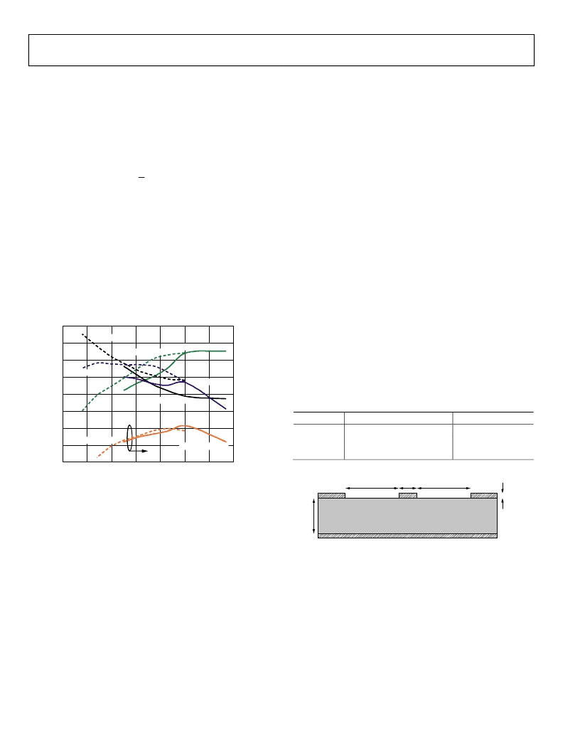
Figure 43 provides a summary of noise, OIP3, IIP3, and SFDR
as a function of device power gain. SFDR is defined as
(
)
S
N
NF
IIP
SFDR
=
3
3
2
where:
IIP3
is the input third-order intercept point, the output
intercept point in dBm minus the gain in dB.
NF
is the noise figure in dB.
N
S
is source resistor noise, –174 dBm for a 1 Hz bandwidth at
300
°
K (27
°C)
.
In general,
N
S
= 10 log
10
(kTB), where k = 1.374 ×10
23
, T is the
temperature in degrees Kelvin, and B is the noise bandwidth in
Hertz.
–30
–20
–10
0
10
20
N
30
40
50
100
110
120
130
140
150
S
160
170
180
–30
–20
–10
0
10
20
30
40
POWER GAIN (dB)
0
SFDR HIGH GAIN
SFDR LOW GAIN
OIP3 HIGH GAIN
OIP3 LOW GAIN
IIP3 LOW GAIN
IIP3 HIGH GAIN
NF HIGH GAIN
NF LOW GAIN
Figure 43. OIP3, IIP3, NF, and SFDR Variation with Gain
As the gain increases, the input amplitude required to deliver
the same output amplitude is reduced. This results in less
distortion at the input stage, and therefore the OIP3 increases.
At some point, the distortion of the input stage becomes small
enough such that the nonlinearity of the output stage becomes
dominant. The OIP3 does not improve significantly as the gain
is increased beyond this point, which explains the knee in the
OIP3 curve. The IIP3 curve has a knee for the same reason;
however, as the gain is increased beyond the knee, the IIP3
starts to decrease rather than increase. This is because in this
region OIP3 is constant, therefore the higher the gain, the lower
the IIP3. The two gain ranges have equal SFDR at approximately
13 dB power gain.
LAYOUT AND OPERATING CONSIDERATIONS
Each input and output pin of the AD8370 presents either a
100 or
50
impedance
relative to their respective ac grounds.
To ensure that signal integrity is not seriously impaired by the
printed circuit board, the relevant connection traces should
provide an appropriate characteristic impedance to the ground
plane. This can be achieved through proper layout.
When laying out an RF trace with a controlled impedance,
consider the following:
Space the ground plane to either side of the signal trace at
least 3 line-widths away to ensure that a microstrip
(vertical dielectric) line is formed, rather than a coplanar
(lateral dielectric) waveguide.
Ensure that the width of the microstrip line is constant and
that there are as few discontinuities as possible , such as
component pads, along the length of the line. Width varia-
tions cause impedance discontinuities in the line and may
result in unwanted reflections.
Do not use silkscreen over the signal line because it alters
the line impedance.
Keep the length of the input and output connection lines
as short as possible.
Figure 44 shows the cross section of a PC board and Table 5
show the dimensions that provide a 100
line impedance for
FR-4 board material with
ε
r
= 4.6.
Table 5.
100
W
22 mils
H
53 mils
T
2 mils
50
13 mils
8 mils
2 mils
W
3W
E
R
3W
H
T
0
Figure 44. Cross-Sectional View of a PC Board
It possible to approximate a 100 trace on a board designed
with the 50 dimensions above by removing the ground plane
within 3 line-widths of the area directly below the trace.
The AD8370 contains both digital and analog sections. Care
should be taken to ensure that the digital and analog sections
are adequately isolated on the PC board. The use of separate
ground planes for each section connected at only one point via
a ferrite bead inductor ensures that the digital pulses do not
adversely affect the analog section of the AD8370.
相關PDF資料 |
PDF描述 |
|---|---|
| AD8370ARE-REEL7 | LF to 750 MHz Digitally Controlled VGA |
| AD8383 | Low Cost 10-Bit, 6-Channel Output Decimating LCD DecDriver |
| AD8383ACPZ | Low Cost 10-Bit, 6-Channel Output Decimating LCD DecDriver |
| AD8391 | xDSL Line Driver 3 V to 12 V with Power-Down |
| AD8391AR | xDSL Line Driver 3 V to 12 V with Power-Down |
相關代理商/技術參數 |
參數描述 |
|---|---|
| AD8370ARE-REEL7 | 功能描述:IC AMP VGA DIFF LN 16TSSOP RoHS:否 類別:集成電路 (IC) >> Linear - Amplifiers - Instrumentation 系列:- 標準包裝:150 系列:- 放大器類型:音頻 電路數:2 輸出類型:- 轉換速率:5 V/µs 增益帶寬積:12MHz -3db帶寬:- 電流 - 輸入偏壓:100nA 電壓 - 輸入偏移:500µV 電流 - 電源:6mA 電流 - 輸出 / 通道:50mA 電壓 - 電源,單路/雙路(±):4 V ~ 32 V,±2 V ~ 16 V 工作溫度:-40°C ~ 85°C 安裝類型:表面貼裝 封裝/外殼:8-TSSOP(0.173",4.40mm 寬) 供應商設備封裝:8-TSSOP 包裝:管件 |
| AD8370AREZ | 功能描述:IC AMP VGA DIFF LN 16TSSOP RoHS:是 類別:集成電路 (IC) >> Linear - Amplifiers - Instrumentation 系列:- 標準包裝:2,500 系列:- 放大器類型:通用 電路數:4 輸出類型:- 轉換速率:0.6 V/µs 增益帶寬積:1MHz -3db帶寬:- 電流 - 輸入偏壓:45nA 電壓 - 輸入偏移:2000µV 電流 - 電源:1.4mA 電流 - 輸出 / 通道:40mA 電壓 - 電源,單路/雙路(±):3 V ~ 32 V,±1.5 V ~ 16 V 工作溫度:0°C ~ 70°C 安裝類型:表面貼裝 封裝/外殼:14-TSSOP(0.173",4.40mm 寬) 供應商設備封裝:14-TSSOP 包裝:帶卷 (TR) 其它名稱:LM324ADTBR2G-NDLM324ADTBR2GOSTR |
| AD8370AREZ | 制造商:Analog Devices 功能描述:IC VARIABLE GAIN AMP 750MHZ TSSOP-16 制造商:Analog Devices 功能描述:IC, VARIABLE GAIN AMP, 750MHZ, TSSOP-16 |
| AD8370AREZ1 | 制造商:AD 制造商全稱:Analog Devices 功能描述:LF to 750 MHz, Digitally Controlled VGA |
| AD8370AREZ-RL7 | 功能描述:IC AMP VGA DIFF LN 16TSSOP RoHS:是 類別:集成電路 (IC) >> Linear - Amplifiers - Instrumentation 系列:- 標準包裝:150 系列:- 放大器類型:音頻 電路數:2 輸出類型:- 轉換速率:5 V/µs 增益帶寬積:12MHz -3db帶寬:- 電流 - 輸入偏壓:100nA 電壓 - 輸入偏移:500µV 電流 - 電源:6mA 電流 - 輸出 / 通道:50mA 電壓 - 電源,單路/雙路(±):4 V ~ 32 V,±2 V ~ 16 V 工作溫度:-40°C ~ 85°C 安裝類型:表面貼裝 封裝/外殼:8-TSSOP(0.173",4.40mm 寬) 供應商設備封裝:8-TSSOP 包裝:管件 |
發布緊急采購,3分鐘左右您將得到回復。