- 您現(xiàn)在的位置:買(mǎi)賣IC網(wǎng) > PDF目錄373945 > AD8370ARE (ANALOG DEVICES INC) LF to 750 MHz Digitally Controlled VGA PDF資料下載
參數(shù)資料
| 型號(hào): | AD8370ARE |
| 廠商: | ANALOG DEVICES INC |
| 元件分類: | 模擬信號(hào)調(diào)理 |
| 英文描述: | LF to 750 MHz Digitally Controlled VGA |
| 中文描述: | SPECIALTY ANALOG CIRCUIT, PDSO16 |
| 封裝: | MO-153ABT, TSSOP-16 |
| 文件頁(yè)數(shù): | 19/28頁(yè) |
| 文件大小: | 1043K |
| 代理商: | AD8370ARE |
第1頁(yè)第2頁(yè)第3頁(yè)第4頁(yè)第5頁(yè)第6頁(yè)第7頁(yè)第8頁(yè)第9頁(yè)第10頁(yè)第11頁(yè)第12頁(yè)第13頁(yè)第14頁(yè)第15頁(yè)第16頁(yè)第17頁(yè)第18頁(yè)當(dāng)前第19頁(yè)第20頁(yè)第21頁(yè)第22頁(yè)第23頁(yè)第24頁(yè)第25頁(yè)第26頁(yè)第27頁(yè)第28頁(yè)
AD8370
ADC INTERFACING
Although the AD8370 is designed to provide a 100 output
source impedance, the device is capable of driving a variety of
loads while maintaining reasonable gain and distortion per-
formance. A common application for the AD8370 is ADC
driving in IF sampling receivers and broadband wide dynamic
range digitizers. The wide gain adjustment range allows the use
of lower resolution ADCs. Figure 52 illustrates a typical ADC
interface network.
Rev. 0 | Page 19 of 28
AD8370
V
OCM
R
OP
100
C
AC
Z
S
R
IP
0
V
IN
V
IN
R
OP
C
AC
Z
S
R
IP
R
T
Z
P
Z
IN
ADC
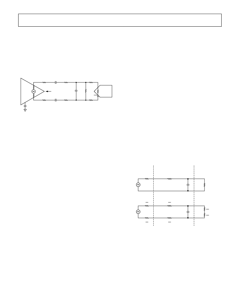
Figure 52. Generic ADC Interface
Many factors need to be considered before defining component
values used in the interface network, such as the desired fre-
quency range of operation, the input swing, and input impedance
of the ADC. AC coupling capacitors, C
AC
, should be used to
block any potential dc offsets present at the AD8370 outputs,
which would otherwise consume the available low-end range of
the ADC. The C
AC
capacitors should be large enough so that
they present negligible reactance over the intended frequency
range of operation. The VOCM pin may serve as an external
reference for ADCs that do not include an on-board reference.
In either case, it is suggested that the VOCM pin be decoupled
to ground through a moderately large bypassing capacitor (1 nF
to 10 nF) to help minimize wideband noise pick-up.
Often it is wise to include input and output parasitic suppression
resistors, R
IP
and R
OP
. Parasitic suppressing resistors help to
prevent resonant effects that occur as a result of internal bond-
wire inductance, pad to substrate capacitance, and stray
capacitance of the printed circuit board trace artwork. If
omitted, undesirable settling characteristics may be observed.
Typically, only 10 to 25 of series resistance is all that is
needed to help dampen resonant effects. Considering that most
ADCs present a relatively high input impedance, very little
signal is lost across the R
IP
and R
OP
series resistors.
Depending on the input impedance presented by the input
system of the ADC, it may be desirable to terminate the ADC
input down to a lower impedance by using a terminating
resistor, R
T
. The high frequency response of the AD8370
exhibits greater peaking when driving very light loads. In
addition, the terminating resistor helps to better define the
input impedance at the ADC input. Any part-to-part variability
of ADC input impedance is reduced when shunting down the
ADC inputs by using a moderate tolerance terminating resistor
(typically a 1% value is acceptable).
After defining reasonable values for coupling capacitors,
suppressing resistors, and the terminating resistor, it is time to
design the intermediate filter network. The example in
Figure 52 suggests a second-order low-pass filter network
comprised of series inductors and a shunt capacitor. The order
and type of filter network used depends on the desired high
frequency rejection required for the ADC interface, as well as
on pass-band ripple and group delay. In some situations, the
signal spectra may already be sufficiently band-limited such
that no additional filter network is necessary, in which case Z
S
would simply be a short and Z
P
would be an open. In other
situations, it may be necessary to have a rather high-order anti-
aliasing filter to help minimize unwanted high frequency
spectra from being aliased down into the first Nyquist zone of
the ADC.
To properly design the filter network, it is necessary to consider
the overall source and load impedance presented by the AD8370
and ADC input, including the additional resistive contribution
of suppression and terminating resistors. The filter design can
then be handled by using a single-ended equivalent circuit as
shown in Figure 53. A variety of references that address filter
synthesis are available. Most provide tables for various filter
types and orders, indicating the normalized inductor and capaci-
tor values for a 1 Hz cutoff frequency and 1 load. After scaling
the normalized prototype element values by the actual desired
cut-off frequency and load impedance, it is simply a matter of
splitting series element reactances in half to realize the final
balanced filter network component values.
V
S
R
S
2
R
S
2
R
L
2
R
L
2
Z
S
2
Z
S
2
Z
P
V
S
R
S
R
L
Z
S
Z
P
SOURCE
LOAD
BALANCED
CONFIGURATION
SINGLE-ENDED
EQUIVALENT
0
Figure 53. Single-Ended-to-Differential Network Conversion
As an example, a second-order Butterworth low-pass filter
design is presented where the differential load impedance is
1200 , and the padded source impedance of the AD8370 is
assumed to be 120 . The normalized series inductor value for
the 10-to-1 load-to-source impedance ratio is 0.074H, and the
normalized shunt capacitor is 14.814 F. For a 70 MHz cutoff
frequency, the single-ended equivalent circuit consists of a
200 nH series inductor followed by a 27 pF capacitor. To realize
the balanced equivalent, simply split the 200 nH inductor in
half to realize the network shown in Figure 54.
相關(guān)PDF資料 |
PDF描述 |
|---|---|
| AD8370ARE-REEL7 | LF to 750 MHz Digitally Controlled VGA |
| AD8383 | Low Cost 10-Bit, 6-Channel Output Decimating LCD DecDriver |
| AD8383ACPZ | Low Cost 10-Bit, 6-Channel Output Decimating LCD DecDriver |
| AD8391 | xDSL Line Driver 3 V to 12 V with Power-Down |
| AD8391AR | xDSL Line Driver 3 V to 12 V with Power-Down |
相關(guān)代理商/技術(shù)參數(shù) |
參數(shù)描述 |
|---|---|
| AD8370ARE-REEL7 | 功能描述:IC AMP VGA DIFF LN 16TSSOP RoHS:否 類別:集成電路 (IC) >> Linear - Amplifiers - Instrumentation 系列:- 標(biāo)準(zhǔn)包裝:150 系列:- 放大器類型:音頻 電路數(shù):2 輸出類型:- 轉(zhuǎn)換速率:5 V/µs 增益帶寬積:12MHz -3db帶寬:- 電流 - 輸入偏壓:100nA 電壓 - 輸入偏移:500µV 電流 - 電源:6mA 電流 - 輸出 / 通道:50mA 電壓 - 電源,單路/雙路(±):4 V ~ 32 V,±2 V ~ 16 V 工作溫度:-40°C ~ 85°C 安裝類型:表面貼裝 封裝/外殼:8-TSSOP(0.173",4.40mm 寬) 供應(yīng)商設(shè)備封裝:8-TSSOP 包裝:管件 |
| AD8370AREZ | 功能描述:IC AMP VGA DIFF LN 16TSSOP RoHS:是 類別:集成電路 (IC) >> Linear - Amplifiers - Instrumentation 系列:- 標(biāo)準(zhǔn)包裝:2,500 系列:- 放大器類型:通用 電路數(shù):4 輸出類型:- 轉(zhuǎn)換速率:0.6 V/µs 增益帶寬積:1MHz -3db帶寬:- 電流 - 輸入偏壓:45nA 電壓 - 輸入偏移:2000µV 電流 - 電源:1.4mA 電流 - 輸出 / 通道:40mA 電壓 - 電源,單路/雙路(±):3 V ~ 32 V,±1.5 V ~ 16 V 工作溫度:0°C ~ 70°C 安裝類型:表面貼裝 封裝/外殼:14-TSSOP(0.173",4.40mm 寬) 供應(yīng)商設(shè)備封裝:14-TSSOP 包裝:帶卷 (TR) 其它名稱:LM324ADTBR2G-NDLM324ADTBR2GOSTR |
| AD8370AREZ | 制造商:Analog Devices 功能描述:IC VARIABLE GAIN AMP 750MHZ TSSOP-16 制造商:Analog Devices 功能描述:IC, VARIABLE GAIN AMP, 750MHZ, TSSOP-16 |
| AD8370AREZ1 | 制造商:AD 制造商全稱:Analog Devices 功能描述:LF to 750 MHz, Digitally Controlled VGA |
| AD8370AREZ-RL7 | 功能描述:IC AMP VGA DIFF LN 16TSSOP RoHS:是 類別:集成電路 (IC) >> Linear - Amplifiers - Instrumentation 系列:- 標(biāo)準(zhǔn)包裝:150 系列:- 放大器類型:音頻 電路數(shù):2 輸出類型:- 轉(zhuǎn)換速率:5 V/µs 增益帶寬積:12MHz -3db帶寬:- 電流 - 輸入偏壓:100nA 電壓 - 輸入偏移:500µV 電流 - 電源:6mA 電流 - 輸出 / 通道:50mA 電壓 - 電源,單路/雙路(±):4 V ~ 32 V,±2 V ~ 16 V 工作溫度:-40°C ~ 85°C 安裝類型:表面貼裝 封裝/外殼:8-TSSOP(0.173",4.40mm 寬) 供應(yīng)商設(shè)備封裝:8-TSSOP 包裝:管件 |
發(fā)布緊急采購(gòu),3分鐘左右您將得到回復(fù)。