- 您現(xiàn)在的位置:買賣IC網(wǎng) > PDF目錄373945 > AD8391AR-REEL (ANALOG DEVICES INC) xDSL Line Driver 3 V to 12 V with Power-Down PDF資料下載
參數(shù)資料
| 型號(hào): | AD8391AR-REEL |
| 廠商: | ANALOG DEVICES INC |
| 元件分類: | 通用總線功能 |
| 英文描述: | xDSL Line Driver 3 V to 12 V with Power-Down |
| 中文描述: | DUAL LINE DRIVER, PDSO8 |
| 封裝: | PLASTIC, SOIC-8 |
| 文件頁數(shù): | 10/20頁 |
| 文件大小: | 278K |
| 代理商: | AD8391AR-REEL |
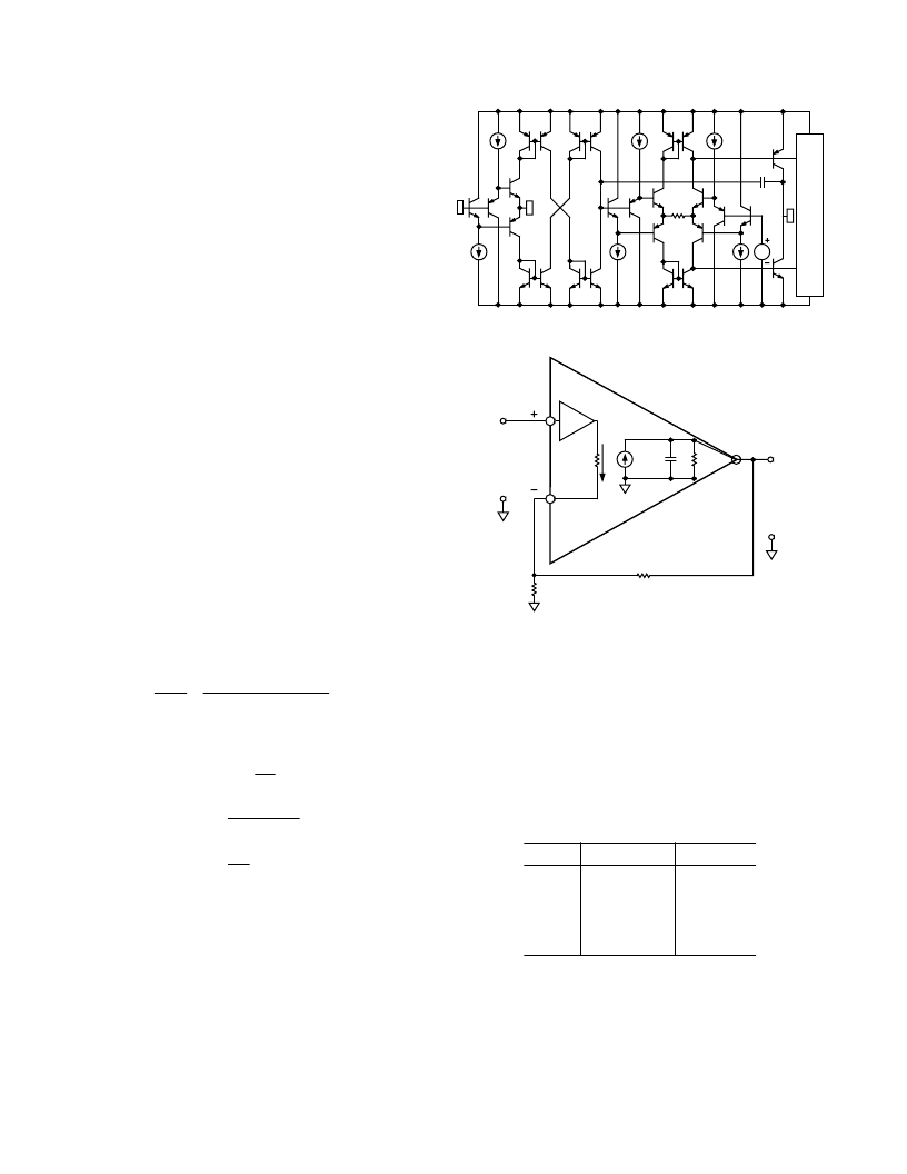
REV. 0
AD8391
–10–
V
O
BIAS
V
N
V
P
Figure 3. Simplified Schematic
G = 1
I
T
= I
IN
C
T
R
T
I
IN
V
OUT
R
G
R
F
R
IN
+
V
IN
–
V
O
+
–
Figure 4. Model of Current Feedback Amplifier
Feedback Resistor Selection
In current feedback amplifiers, selection of the feedback and
gain resistors will impact distortion, bandwidth,
noise, and gain
flatness. Care should be exercised in the selection
of these resistors
so that the optimum performance is achieved. Table I shows the
recommended resistor values for use in a
variety of gain settings for
the test circuits in TPC 1 and TPC 19.
These values are only
intended to be a starting point when designing for any application.
Table I. Resistor Selection Guide
Gain
R
F
( )
909
909
909
909
909
R
G
( )
909
453
303
227
178
–
1
–
2
–
3
–
4
–
5
GENERAL INFORMATION
Theory of Operation
The AD8391 is a dual current feedback amplifier with high
output current capability. It is fabricated on Analog Devices
’
proprietary eXtra Fast Complementary Bipolar Process (XFCB)
that
enables the construction of PNP and NPN transistors with f
T
’
s
greater than 3 GHz. The process uses dielectrically isolated
transistors to eliminate the parasitic and latch-up problems caused
by junction
isolation. These features enable the construction of
high-frequency,
low-distortion amplifiers.
The AD8391 has a unique pin out. The two noninverting inputs
of the amplifier are connected to the V
MID
pin, which is internally
biased by two 5 k
resistors forming a voltage divider between
+V
S
and
–
V
S
. V
MID
is accessible through Pin 7. There is also a
10 pF internal capacitor from V
MID
to
–
V
S.
The two inverting pins
are available at Pin 1 and Pin 8, allowing the gain of the amplifiers to
be set with external resistors
. See the front page for a connection
diagram of the AD8391.
A simplified schematic of an amplifier is shown in Figure 3. Emitter
followers buffer the positive input, V
P
, to provide low-input current
and current noise. The low-impedance current feedback summing
junction is at the negative input, V
N
. The output stage is another
high-gain amplifier used as an integrator to provide frequency com-
pensation. The complementary common-emitter output provides the
extended output swing.
A current feedback amplifier
’
s bandwidth and distortion
performance are relatively insensitive to its closed-loop signal gain,
which is a distinct advantage over a voltage-feedback architecture.
Figure 4 shows a simplified model of a current feedback amplifier.
The feedback signal is an error current that flows into the inverting
node. R
IN
is inversely proportional to the transconductance of
the amplifier
’
s input stage, g
mi
. Circuit analysis of the pictured
follower with gain circuit yields:
V
V
G
Tz s
+
Tz s
R
G
R
OUT
IN
F
IN
=
×
+
×
where:
G
R
R
F
G
= +
1
Tz s
R
sC
R
F
T
T
=
+
1
(
)
R
g
IN
mi
=
1
125
Recognizing that G
×
R
IN
<<
R
F
, and that the
–
3 dB point is set
when
Tz(s)
=
R
F
, one can see that the amplifier
’
s bandwidth
depends primarily on the feedback resistor. There is a value of
R
F
below which the amplifier will be unstable, as the
amplifier
will have additional poles that will contribute excess phase shift.
The optimum value for R
F
depends on the gain and the amount
of peaking tolerable in the application. For more
information
about current feedback amplifiers, see ADI
’
s High-Speed Design
Techniques at www.analog.com/technology/amplifiersLinear/
designTools/evaluationBoards/pdf/1.pdf
.
相關(guān)PDF資料 |
PDF描述 |
|---|---|
| AD8391AR-REEL7 | xDSL Line Driver 3 V to 12 V with Power-Down |
| AD8392ARE-REEL | Low Power, High Output Current, Quad Op Amp, Dual-Channel ADSL/ADSL2+ Line Driver |
| AD8392ARE-REEL7 | Low Power, High Output Current, Quad Op Amp, Dual-Channel ADSL/ADSL2+ Line Driver |
| AD8392 | Low Power, High Output Current, Quad Op Amp, Dual-Channel ADSL/ADSL2+ Line Driver |
| AD8392ACP-R2 | Low Power, High Output Current, Quad Op Amp, Dual-Channel ADSL/ADSL2+ Line Driver |
相關(guān)代理商/技術(shù)參數(shù) |
參數(shù)描述 |
|---|---|
| AD8391AR-REEL7 | 功能描述:IC XDSL LINE DVR W/PWR DN 8-SOIC RoHS:否 類別:集成電路 (IC) >> 接口 - 驅(qū)動(dòng)器,接收器,收發(fā)器 系列:- 標(biāo)準(zhǔn)包裝:1,140 系列:AU 類型:收發(fā)器 驅(qū)動(dòng)器/接收器數(shù):1/1 規(guī)程:CAN 電源電壓:5.3 V ~ 27 V 安裝類型:表面貼裝 封裝/外殼:14-SOIC(0.154",3.90mm 寬) 供應(yīng)商設(shè)備封裝:14-SO 包裝:管件 其它名稱:935267940512AU5790D14AU5790D14-ND |
| AD8391ARZ | 制造商:Analog Devices 功能描述:SP Amp Line Driver Amp Dual ±6V/12V 8-Pin SOIC N Tube |
| AD8392 | 制造商:AD 制造商全稱:Analog Devices 功能描述:Low Power, High Output Current, Quad Op Amp, Dual-Channel ADSL/ADSL2+ Line Driver |
| AD8392A | 制造商:AD 制造商全稱:Analog Devices 功能描述:Low Power, High Output Current, Quad Op Amp, Dual-Channel ADSL/ADSL2+ Line Driver |
| AD8392AACPZ-R2 | 制造商:Analog Devices 功能描述:ADSL Driver Quad 32-Pin LFCSP EP T/R 制造商:Analog Devices 功能描述:ADSL DRVR QUAD 32LFCSP EP - Tape and Reel |
發(fā)布緊急采購(gòu),3分鐘左右您將得到回復(fù)。