- 您現(xiàn)在的位置:買賣IC網(wǎng) > PDF目錄373946 > AD8402 (Analog Devices, Inc.) 2-Channel, 256-Position Digital Potentiometer PDF資料下載
參數(shù)資料
| 型號(hào): | AD8402 |
| 廠商: | Analog Devices, Inc. |
| 元件分類: | 數(shù)字電位計(jì) |
| 英文描述: | 2-Channel, 256-Position Digital Potentiometer |
| 中文描述: | 2通道,256位數(shù)字電位器 |
| 文件頁數(shù): | 13/20頁 |
| 文件大小: | 496K |
| 代理商: | AD8402 |
AD8400/AD8402/AD8403
REV. B
–13–
where Dx is the data contained in the 8-bit RDAC# latch, and
R
BA
is the nominal end-to-end resistance. For example, when
V
A
= 0 V and B terminal is open circuit, the following output
resistance values will be set for the following RDAC latch codes
(applies to 10 k
potentiometers):
D
(Dec)
R
WA
(
)
Output State
255
128
1
0
89
5050
10011
10050
Full Scale
Midscale (
RS
= 0 Condition)
1 LSB
Zero Scale
The typical distribution of R
BA
from channel-to-channel matches
within
±
1%. However, device-to-device matching is process lot
dependent having a
±
20% variation. The change in R
BA
with
temperature has a positive 500 ppm/
°
C temperature coefficient.
The wiper-to-end-terminal resistance temperature coefficient
has the best performance over the 10% to 100% of adjustment
range where the internal wiper contact switches do not contribute
any significant temperature related errors. The graph in Figure
11 shows the performance of R
WB
tempco vs. code, using the
trimmer with codes below 32 results in the larger temperature
coefficients plotted.
PROGRAMMING THE POTENTIOMETER DIVIDER
Voltage Output Operation
The digital potentiometer easily generates an output voltage
proportional to the input voltage applied to a given terminal.
For example, connecting A terminal to +5 V and B terminal to
ground produces an output voltage at the wiper starting at zero
volts up to 1 LSB less than +5 V. Each LSB of voltage is equal
to the voltage applied across terminal AB divided by the 256
position resolution of the potentiometer divider. The general
equation defining the output voltage with respect to ground for
any given input voltage applied to terminals AB is:
V
W
(
Dx
) =
Dx
/256
×
V
AB
+
V
B
Operation of the digital potentiometer in the divider mode re-
sults in more accurate operation over temperature. Here the
output voltage is dependent on the ratio of the internal resistors,
not the absolute value; therefore, the temperature drift improves
to 15 ppm/
°
C.
At the lower wiper position settings, the potentiometer divider
temperature coefficient increases due to the contributions of the
CMOS switch wiper resistance becoming an appreciable portion
of the total resistance from terminal B to the wiper. See Figure 10
for a plot of potentiometer tempco performance versus code
setting.
Equation 4
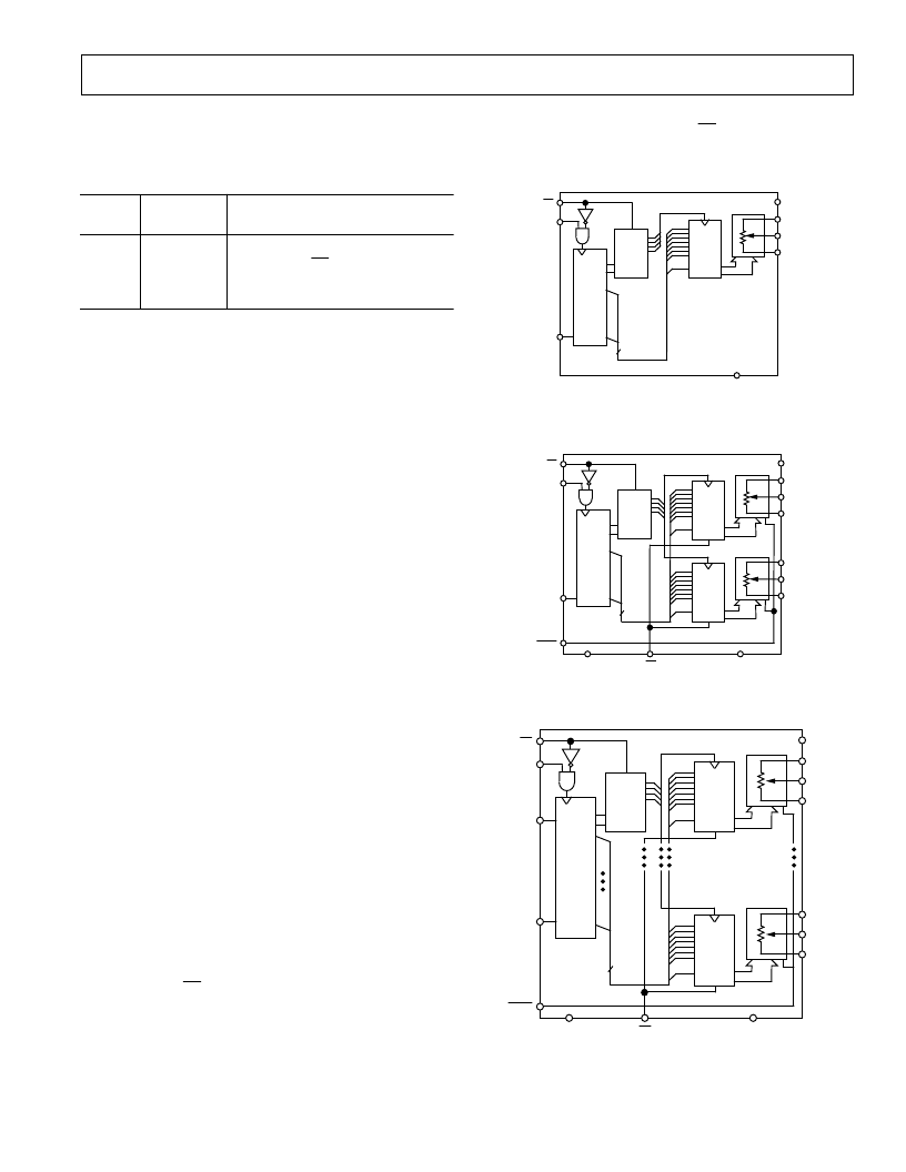
DIGITAL INTERFACING
The AD8400/AD8402/AD8403 contains a standard SPI com-
patible three-wire serial input control interface. The three inputs
are clock (CLK),
CS
and serial data input (SDI). The positive-
edge sensitive CLK input requires clean transitions to avoid
clocking incorrect data into the serial input register. For best re-
sults use logic transitions faster than 1 V/
μ
s. Standard logic
families work well. If mechanical switches are used for product
evaluation, they should be debounced by a flip-flop or other
suitable means. The Figure 38 block diagrams show more detail
of the internal digital circuitry. When
CS
is taken active low, the
clock loads data into the 10-bit serial register on each positive
clock edge (see Table II).
R
DAC
LAT
#1
GND
A1
W1
B1
V
DD
AD8400
CS
CLK
8
D7
D0
EN
DEC
A1
A0
SDI
DI
REG
D0
D7
SER
a.
R
DAC
LAT
#1
R
AGND
RS
A1
W1
B1
V
DD
AD8402
CS
CLK
8
D7
D0
R
DAC
LAT
#2
R
A4
W4
B4
D7
D0
EN
ADDR
DEC
A1
A0
SDI
DI
1SER
REG
D0
SHDN
DGND
D7
b.
R
DAC
LAT
#1
R
AGND
RS
A1
W1
B1
V
DD
AD8403
CS
CLK
SDO
8
D7
D0
R
DAC
LAT
#4
R
A4
W4
B4
D7
D0
EN
ADDR
DEC
A1
A0
D7
SDI
DO
DI
SER
REG
D0
SHDN
DGND
c.
Figure 38. Block Diagrams
相關(guān)PDF資料 |
PDF描述 |
|---|---|
| AD8402AN1 | 32-Tap. Nonvolatile. Linear-Taper Digital Potentiometers in SOT23 |
| AD8402AN10 | 32-Tap. Nonvolatile. Linear-Taper Digital Potentiometers in SOT23 |
| AD8402AN100 | 32-Tap. Nonvolatile. Linear-Taper Digital Potentiometers in SOT23 |
| AD8402AN50 | 32-Tap. Nonvolatile. Linear-Taper Digital Potentiometers in SOT23 |
| AD8402AR1 | 32-Tap. Nonvolatile. Linear-Taper Digital Potentiometers in SOT23 |
相關(guān)代理商/技術(shù)參數(shù) |
參數(shù)描述 |
|---|---|
| AD8402AN1 | 制造商:Rochester Electronics LLC 功能描述:DUAL 8-BIT POTENTIOMETER 1K OHM - Bulk |
| AD8402AN10 | 功能描述:IC DGTL POT 8BIT 10K 2CH 14-DIP RoHS:否 類別:集成電路 (IC) >> 數(shù)據(jù)采集 - 數(shù)字電位器 系列:- 標(biāo)準(zhǔn)包裝:3,000 系列:DPP 接片:32 電阻(歐姆):10k 電路數(shù):1 溫度系數(shù):標(biāo)準(zhǔn)值 300 ppm/°C 存儲(chǔ)器類型:非易失 接口:3 線串行(芯片選擇,遞增,增/減) 電源電壓:2.5 V ~ 6 V 工作溫度:-40°C ~ 85°C 安裝類型:表面貼裝 封裝/外殼:8-WFDFN 裸露焊盤 供應(yīng)商設(shè)備封裝:8-TDFN(2x3) 包裝:帶卷 (TR) |
| AD8402AN100 | 制造商:Rochester Electronics LLC 功能描述:DUAL 8-BIT POTENTIOMETER - Bulk 制造商:Analog Devices 功能描述:SEMICONDUCTORSLINEAR |
| AD8402AN50 | 制造商:Rochester Electronics LLC 功能描述:DUAL 8-BIT POTENTIOMETER - Bulk |
| AD8402-AN50 | 制造商:Analog Devices 功能描述: |
發(fā)布緊急采購(gòu),3分鐘左右您將得到回復(fù)。