- 您現(xiàn)在的位置:買賣IC網(wǎng) > PDF目錄373946 > AD841SQ (ANALOG DEVICES INC) Wideband, Unity-Gain Stable, Fast Settling Op Amp PDF資料下載
參數(shù)資料
| 型號: | AD841SQ |
| 廠商: | ANALOG DEVICES INC |
| 元件分類: | 運(yùn)動控制電子 |
| 英文描述: | Wideband, Unity-Gain Stable, Fast Settling Op Amp |
| 中文描述: | OP-AMP, 5500 uV OFFSET-MAX, 40 MHz BAND WIDTH, CDIP14 |
| 封裝: | HERMETIC SEALED, CERDIP-14 |
| 文件頁數(shù): | 2/8頁 |
| 文件大小: | 354K |
| 代理商: | AD841SQ |
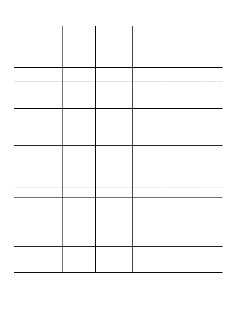
AD841–SPECIFICATIONS
Model
AD841J
Typ
AD841K
Min
AD841S
1
Typ
Conditions
Min
Max
Typ
Max
Min
Max
Units
INPUT OFFSET VOLTAGE
2
0.8
2.0
5.0
0.5
1.0
3.3
0.5
2.0
5.5
mV
mV
μ
V/
°
C
μ
A
μ
A
μ
A
μ
A
T
MIN
–T
MAX
Offset Drift
35
35
35
INPUT BIAS CURRENT
3.5
8
10
0.4
0.5
3.5
5
6
0.2
0.3
3.5
8
12
0.4
0.6
T
MIN
–T
MAX
Input Offset Current
0.1
0.1
0.1
T
MIN
–T
MAX
Differential Mode
INPUT CHARACTERISTICS
Input Resistance
Input Capacitance
200
2
200
2
200
2
k
pF
INPUT VOLTAGE RANGE
Common Mode
Common-Mode Rejection
6
10
86
80
12
100
6
10
103
100
12
109
6
10
86
80
12
110
V
dB
dB
nV/
√
Hz
μ
V rms
V
CM
=
±
10 V
T
MIN
–T
MAX
f = 1 kHz
10 Hz to 10 MHz
V
O
=
±
10 V
R
LOAD
≥
500
T
MIN
–T
MAX
INPUT VOLTAGE NOISE
Wideband Noise
15
47
15
47
15
47
OPEN-LOOP GAIN
25
12
45
25
20
45
25
12
45
V/mV
V/mV
OUTPUT CHARACTERISTICS
Voltage
R
LOAD
≥
500
T
MIN
–T
MAX
V
OUT
=
±
10 V
±
10
50
±
10
50
±
10
50
V
mA
Current
OUTPUT RESISTANCE
Open Loop
5
5
5
FREQUENCY RESPONSE
Unity Gain Bandwidth
Full Power Bandwidth
3
V
OUT
= 90 mV p-p
V
O
= 20 V p-p
R
LOAD
≥
500
A
V
= –1
A
V
= –1
A
V
= –1
A
V
= –1
to 0.1%
to 0.01%
40
40
40
MHz
3.1
4.7
10
10
300
3.1
4.7
10
10
300
3.1
4.7
10
10
300
MHz
ns
%
V/
μ
s
Rise Time
4
Overshoot
4
Slew Rate
4
Settling Time – 10 V Step
200
200
200
90
110
00
110
90
110
ns
ns
OVERDRIVE RECOVERY
–Overdrive
+Overdrive
200
700
200
700
200
700
ns
ns
DIFFERENTIAL GAIN
Differential Phase
f = 4.4 MHz
f = 4.4 MHz
0.03
0.022
0.03
0.022
0.03
0.022
%
Degree
POWER SUPPLY
Rated Performance
Operating Range
Quiescent Current
±
15
±
15
±
15
V
V
mA
mA
dB
dB
±
5
±
18
12
14
±
5
±
18
12
14
±
5
±
18
12
16
11
11
11
T
MIN
–T
MAX
V
S
=
±
5 V to
±
18 V
T
MIN
–T
MAX
Power Supply Rejection Ratio
86
80
100
90
86
100
86
80
100
TEMPERATURE RANGE
Rated Performance
5
0
+75
0
+75
–55
+125
°
C
PACKAGE OPTIONS
LCC (E-20A)
Cerdip (Q-14)
Plastic (N-14)
TO-8 (H-12)
Chips
AD841SE, AD841SE/883B
AD841SQ, AD841SQ/883B
AD841JQ
AD841JN
AD841JH
AD841J CHIPS
AD841KQ
AD841KN
AD841KH
AD841SH, AD841SH/883B
AD841S CHIPS
NOTES
1
Standard Military Drawing Available: 5962-89641012A – (SE/883B); 5962-8964101CA – (SQ/883B).
2
Input offset voltage specifications are guaranteed after 5 minutes at T
A
= +25
°
C.
3
Full power bandwidth = Slew Rate/2
π
V
PEAK
.
3
Refer to Figure 19.
4
“S” grade T
MIN
–T
MAX
specifications are tested with automatic test equipment at T
A
= –55
°
C and T
A
= +125
°
C.
All min and max specifications are guaranteed. Specifications shown in
boldface
are tested on all production units.
Specifications subject to change without notice.
REV. B
–2–
(@ +25
8
C and
6
15 V dc, unless otherwise noted)
相關(guān)PDF資料 |
PDF描述 |
|---|---|
| AD841JQ | Wideband, Unity-Gain Stable, Fast Settling Op Amp |
| AD841KQ | Wideband, Unity-Gain Stable, Fast Settling Op Amp |
| AD847A | High Speed, Low Power Monolithic Op Amp |
| AD847J | High Speed, Low Power Monolithic Op Amp |
| AD847S | High Speed, Low Power Monolithic Op Amp |
相關(guān)代理商/技術(shù)參數(shù) |
參數(shù)描述 |
|---|---|
| AD841SQ/883B | 功能描述:高速運(yùn)算放大器 FAST SETTLING H.S. OP AMP RoHS:否 制造商:Texas Instruments 通道數(shù)量:1 電壓增益 dB:116 dB 輸入補(bǔ)償電壓:0.5 mV 轉(zhuǎn)換速度:55 V/us 工作電源電壓:36 V 電源電流:7.5 mA 最大工作溫度:+ 85 C 安裝風(fēng)格:SMD/SMT 封裝 / 箱體:SOIC-8 封裝:Tube 產(chǎn)品: |
| AD842 | 制造商:AD 制造商全稱:Analog Devices 功能描述:Wideband, High Output Current, Fast Settling Op Amp |
| AD8420 | 制造商:AD 制造商全稱:Analog Devices 功能描述:Low Noise, Low Gain Drift, G = 2000 |
| AD8420_12 | 制造商:AD 制造商全稱:Analog Devices 功能描述:Wide Supply Range, Micropower, |
發(fā)布緊急采購,3分鐘左右您將得到回復(fù)。