- 您現在的位置:買賣IC網 > PDF目錄373947 > AD8512 (Analog Devices, Inc.) Precision, Very Low Noise, Low Input Bias Current, Wide Bandwidth JFET Operational Amplifiers PDF資料下載
參數資料
| 型號: | AD8512 |
| 廠商: | Analog Devices, Inc. |
| 英文描述: | Precision, Very Low Noise, Low Input Bias Current, Wide Bandwidth JFET Operational Amplifiers |
| 中文描述: | 精密,非常低噪聲,低輸入偏置電流,高帶寬結型場效應管運算放大器 |
| 文件頁數: | 17/20頁 |
| 文件大小: | 497K |
| 代理商: | AD8512 |
AD8510/AD8512/AD8513
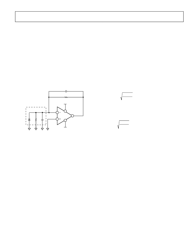
I-V CONVERSION APPLICATIONS
Photodiode Circuits
Common applications for I-V conversion include photodiode
circuits, where the amplifier is used to convert a current emitted
by a diode placed at the positive input terminal into an output
voltage.
Rev. E | Page 17 of 20
The AD8510/AD8512/AD8513’s low input bias current, wide
bandwidth, and low noise make them each an excellent choice
for various photodiode applications, including fax machines,
fiber optic controls, motion sensors, and bar code readers.
The circuit shown in Figure 53 uses a silicon diode with zero
bias voltage. This is known as a Photovoltaic Mode; this
configuration limits the overall noise and is suitable for
instrumentation applications.
4
7
3
6
2
AD8510
Cf
R2
Rd
Ct
V
EE
V
CC
0
Figure 53. Equivalent Preamplifier Photodiode Circuit
A larger signal bandwidth can be attained at the expense of
additional output noise. The total input capacitance (Ct)
consists of the sum of the diode capacitance (typically 3 pF to
4 pF) and the amplifier’s input capacitance (12 pF), which
includes external parasitic capacitance. Ct creates a pole in the
frequency response, which may lead to an unstable system. To
ensure stability and optimize the bandwidth of the signal, a
capacitor is placed in the feedback loop of the circuit shown in
Figure 53. It creates a zero and yields a bandwidth whose corner
frequency is 1/(2π(R2Cf)).
The value of
R
2 can be determined by the ratio V/I
D
, where V is
the desired output voltage of the op amp and I
D
is the diode
current. For example, if I
D
is 100 μA and a 10 V output voltage is
desired, R2 should be 100 k. Rd is a junction resistance that
drops typically by a factor of 2 for every 10°C increase in
temperature. A typical value for Rd is 1000 M. Since Rd >> R2,
the circuit behavior is not impacted by the effect of the junction
resistance. The maximum signal bandwidth is
Ct
2
R
ft
f
MAX
2
π
=
where f
t
is the unity gain frequency of the amplifier.
Using the parameters above,
Cf
≈ 1 pF, which yields a signal
bandwidth of about 2.6 MHz.
ft
R
Ct
Cf
2
2
π
=
where
ft
is the unity gain frequency of the op amp, achieves a
phase margin, Φ
m
, of approximately 45°.
A higher phase margin can be obtained by increasing the value
of
Cf
. Setting
Cf
to twice the previous value yields approximately
Φ
m
= 65° and a maximally flat frequency response, but reduces
the maximum signal bandwidth by 50%.
相關PDF資料 |
PDF描述 |
|---|---|
| AD8512AR | Precision, Very Low Noise, Low Input Bias Current, Wide Bandwidth JFET Operational Amplifiers |
| AD8512AR-REEL | Precision, Very Low Noise, Low Input Bias Current, Wide Bandwidth JFET Operational Amplifiers |
| AD8510ARZ-REEL | Precision, Very Low Noise, Low Input Bias Current, Wide Bandwidth JFET Operational Amplifiers |
| AD8522 | +5 Volt, Serial Input,Dual 12-Bit DAC(串行輸入,雙12位D/A轉換器) |
| AD8531AKS | Precision, Quad, SPST Analog Switches |
相關代理商/技術參數 |
參數描述 |
|---|---|
| AD85-12/883B | 制造商:Analog 功能描述:_ |
| AD8512883B | 制造商:Analog 功能描述:_ |
| AD8512AR | 功能描述:IC OPAMP JFET 8MHZ DUAL LN 8SOIC RoHS:否 類別:集成電路 (IC) >> Linear - Amplifiers - Instrumentation 系列:- 標準包裝:1 系列:- 放大器類型:通用 電路數:4 輸出類型:滿擺幅 轉換速率:0.6 V/µs 增益帶寬積:1MHz -3db帶寬:- 電流 - 輸入偏壓:2pA 電壓 - 輸入偏移:1000µV 電流 - 電源:85µA 電流 - 輸出 / 通道:20mA 電壓 - 電源,單路/雙路(±):1.8 V ~ 6 V 工作溫度:-40°C ~ 125°C 安裝類型:表面貼裝 封裝/外殼:14-SOIC(0.154",3.90mm 寬) 供應商設備封裝:14-SOICN 包裝:剪切帶 (CT) 產品目錄頁面:680 (CN2011-ZH PDF) 其它名稱:MCP6L04T-E/SLCT |
| AD8512ARM-R2 | 制造商:Analog Devices 功能描述:OP Amp Dual GP 制造商:Analog Devices 功能描述:IC AMP LOW NOISE |
| AD8512ARM-REEL | 制造商:Analog Devices 功能描述:OP AMP DUAL GP 15V 8MSOP - Tape and Reel 制造商:Analog Devices 功能描述:IC AMP LOW NOISE |
發布緊急采購,3分鐘左右您將得到回復。