- 您現在的位置:買賣IC網 > PDF目錄373947 > AD8522 (Analog Devices, Inc.) +5 Volt, Serial Input,Dual 12-Bit DAC(串行輸入,雙12位D/A轉換器) PDF資料下載
參數資料
| 型號: | AD8522 |
| 廠商: | Analog Devices, Inc. |
| 英文描述: | +5 Volt, Serial Input,Dual 12-Bit DAC(串行輸入,雙12位D/A轉換器) |
| 中文描述: | 5伏,串行輸入,雙12位DAC(串行輸入,雙12位的D / A轉換器) |
| 文件頁數: | 5/8頁 |
| 文件大小: | 189K |
| 代理商: | AD8522 |
AD8522
REV. A
–5–
OPE RAT ION
T he AD8522 is a complete ready-to-use dual 12-bit digital-to-
analog converter. Only one +5 V power supply is necessary for
operation. It contains two voltage-switched, 12-bit, laser-
trimmed digital-to-analog converters, a curvature-corrected
bandgap reference, rail-to-rail output op amps, input registers,
and DAC registers. T he serial data interface consists of a serial
data input (SDI), clock (CLK ), and two load strobe pins (
LDA
,
LDB
) with an active low
CS
strobe. In addition, an asynchro-
nous
RS
pin will set all DAC register bits to zero causing the
V
OUT
to become zero volts, or to midscale for trimming applica-
tions when the MSB pin is programmed to Logic 1. T his func-
tion is useful for power on reset or system failure recovery to a
known state.
D/A CONVE RT E R SE CT ION
T he internal DAC is a 12-bit voltage-mode device with an out-
put that swings from AGND potential to the 2.5 V internal
bandgap voltage. It uses a laser-trimmed R-2R ladder which is
switched by N channel MOSFET s. T he output voltage of the
DAC has a constant resistance independent of digital input
code. T he DAC output is internally connected to the rail-to-rail
output op amp.
AMPLIFIE R SE CT ION
T he internal DAC’s output is buffered by a low power con-
sumption precision amplifier. T his low power amplifier contains
a differential PNP pair input stage that provides low offset volt-
age and low noise, as well as the ability to amplify the zero-scale
DAC output voltages. T he rail-to-rail amplifier is configured in
a gain of 1.638 (= 4.095 V/2.5 V) in order to set the 4.095 V
full-scale output (1 mV/LSB). See Figure 4 for an equivalent
circuit schematic of the analog section.
BUFFER
2R
2R
2R
2R
R
R
SPDT
N CH FET
SWITCHES
2R
R2
R1
RAIL-TO-RAIL
OUTPUT
AMPLIFIER
V
OUT
BANDGAP
REFERENCE
V
2.5V
VOLTAGE SWITCHED 12-BIT
R-2R D/A CONVERTER
A
= 4.096/2.5
= 1.638V/V
Figure 4. Equivalent AD8522 Schematic of Analog Portion
T he op amp has a 16
μ
s typical settling time to 0.01%. T here
are slight differences in settling time for negative slewing signals
versus positive. See the oscilloscope photos in the “T ypical Per-
formance Characteristics” section of this data sheet.
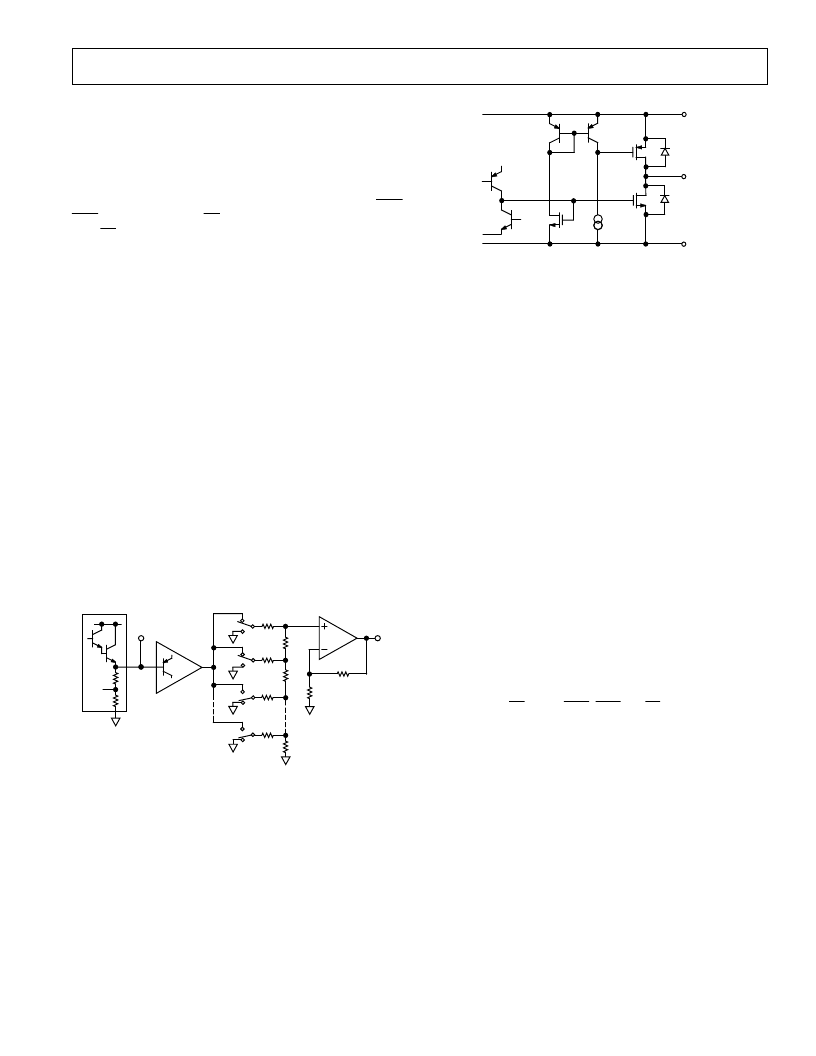
OUT PUT SE CT ION
T he rail-to-rail output stage of this amplifier has been designed
to provide precision performance while operating near either
power supply. Figure 5 shows an equivalent output schematic of
the rail-to-rail amplifier with its N channel pull-down FET s that
will pull an output load directly to GND. T he output sourcing
current is provided by a P channel pull-up device that can sup-
ply GND terminated loads, especially important at the –10%
supply tolerance value of 4.5 V.
P-CH
N-CH
V
DD
V
OUT
AGND
Figure 5. Equivalent Analog Output Circuit
Figures 6 and 7 in the typical performance characteristics sec-
tion provide information on output swing performance near
ground and full scale as a function of load. In addition to resis-
tive load driving capability the amplifier has also been carefully
designed and characterized for up to 500 pF capacitive load
driving capability.
RE FE RE NCE SE CT ION
T he internal 2.5 V curvature-corrected bandgap voltage refer-
ence is laser trimmed for both initial accuracy and low tempera-
ture coefficient. T he voltage generated by the reference is
available at the V
REF
pin. Since V
REF
is
not
intended to drive
heavy external loads, it must be buffered. T he equivalent emit-
ter follower output circuit of the V
REF
pin is shown in Figure 4.
Bypassing the V
REF
pin will improve noise performance; how-
ever, bypassing is not required for proper operation. Figure 10
shows broad band noise performance.
POWE R SUPPLY
T he very low power consumption of the AD8522 is a direct
result of a circuit design optimizing use of a CBCMOS process.
By using the low power characteristics of the CMOS for the
logic, and the low noise, tight matching of the complementary
bipolar transistors good analog accuracy is achieved.
For power consumption sensitive applications it is important to
note that the internal power consumption of the AD8522 is
strongly dependent on the actual in
put voltage levels present on
the SDI, CLK ,
CS
, MSB,
LDA
,
LDB
and
RS
pins. Since these in-
puts are standard CMOS logic structures, they contribute static
power dissipation dependent on the actual driving logic V
OH
and
V
OL
voltage levels. Consequently for optimum dissipation use of
CMOS logic versus T T L provides minimal dissipation in the static
state. A V
INL
= 0 V on the logic input pins provides the lowest
standby dissipation of 1 mA with a +5 V power supply.
As with any analog system, it is recommended that the AD8522
power supply be bypassed on the same PC card that contains
the chip. Figure 12 shows the power supply rejection versus fre-
quency performance. T his should be taken into account when
using higher frequency switched-mode power supplies with
ripple frequencies of 100 kHz and higher.
One advantage of the rail-to-rail output amplifiers used in the
AD8522 is the wide range of usable supply voltage. T he part is
fully specified and tested over temperature for operation from
+4.5 V to +5.5 V. If reduced linearity and source current capa-
bility near full scale can be tolerated, operation of the AD8522
相關PDF資料 |
PDF描述 |
|---|---|
| AD8531AKS | Precision, Quad, SPST Analog Switches |
| AD8531AR | Low Cost, 250 mA Output Single-Supply Amplifiers |
| AD8531ART | Low Cost, 250 mA Output Single-Supply Amplifiers |
| AD8531 | Low Cost, 250 mA Output Single-Supply Amplifiers(低成本,250mA輸出,單電源放大器) |
| AD8532 | Low Cost, 250 mA Output Single-Supply Amplifiers(低成本,250mA輸出,單電源雙放大器) |
相關代理商/技術參數 |
參數描述 |
|---|---|
| AD8522ACPZ-REEL | 功能描述:IC DAC DUAL 12BIT 5V 制造商:analog devices inc. 系列:- 零件狀態:上次購買時間 標準包裝:1 |
| AD8522ACPZ-REEL7 | 功能描述:IC DAC DUAL 12BIT 5V 制造商:analog devices inc. 系列:- 零件狀態:上次購買時間 標準包裝:1 |
| AD8522AN | 功能描述:IC DAC DUAL 12BIT 5V 14-DIP RoHS:否 類別:集成電路 (IC) >> 數據采集 - 數模轉換器 系列:- 產品培訓模塊:Data Converter Fundamentals DAC Architectures 標準包裝:750 系列:- 設置時間:7µs 位數:16 數據接口:并聯 轉換器數目:1 電壓電源:雙 ± 功率耗散(最大):100mW 工作溫度:0°C ~ 70°C 安裝類型:表面貼裝 封裝/外殼:28-LCC(J 形引線) 供應商設備封裝:28-PLCC(11.51x11.51) 包裝:帶卷 (TR) 輸出數目和類型:1 電壓,單極;1 電壓,雙極 采樣率(每秒):143k |
| AD8522AN | 制造商:Analog Devices 功能描述:SEMICONDUCTORSLINEAR |
| AD8522ANZ | 功能描述:IC DAC DUAL 12BIT 5V 14DIP RoHS:是 類別:集成電路 (IC) >> 數據采集 - 數模轉換器 系列:- 產品培訓模塊:Data Converter Fundamentals DAC Architectures 標準包裝:750 系列:- 設置時間:7µs 位數:16 數據接口:并聯 轉換器數目:1 電壓電源:雙 ± 功率耗散(最大):100mW 工作溫度:0°C ~ 70°C 安裝類型:表面貼裝 封裝/外殼:28-LCC(J 形引線) 供應商設備封裝:28-PLCC(11.51x11.51) 包裝:帶卷 (TR) 輸出數目和類型:1 電壓,單極;1 電壓,雙極 采樣率(每秒):143k |
發布緊急采購,3分鐘左右您將得到回復。