- 您現在的位置:買賣IC網 > PDF目錄373950 > AD8571ARM (ANALOG DEVICES INC) Zero-Drift, Single-Supply, Rail-to-Rail Input/Output Operational Amplifiers PDF資料下載
參數資料
| 型號: | AD8571ARM |
| 廠商: | ANALOG DEVICES INC |
| 元件分類: | 運動控制電子 |
| 英文描述: | Zero-Drift, Single-Supply, Rail-to-Rail Input/Output Operational Amplifiers |
| 中文描述: | OP-AMP, 10 uV OFFSET-MAX, 1 MHz BAND WIDTH, PDSO8 |
| 封裝: | MSOP-8 |
| 文件頁數: | 14/19頁 |
| 文件大小: | 247K |
| 代理商: | AD8571ARM |
AD8571/AD8572/AD8574
–14–
REV. 0
Input Overvoltage Protection
Although the AD857x is a rail-to-rail input amplifier, care should
be taken to ensure that the potential difference between the inputs
does not exceed 5 V. Under normal operating conditions, the
amplifier will correct its output to ensure the two inputs are at
the same voltage. However, if the device is configured as a com-
parator, or is under some unusual operating condition, the input
voltages may be forced to different potentials. This could cause
excessive current to flow through internal diodes in the AD857x
used to protect the input stage against overvoltage.
If either input exceeds either supply rail by more than 0.3 V, large
amounts of current will begin to flow through the ESD protection
diodes in the amplifier. These diodes are connected between the
inputs and each supply rail to protect the input transistors against
an electrostatic discharge event and are normally reverse-biased.
However, if the input voltage exceeds the supply voltage, these
ESD diodes will become forward-biased. Without current-limiting,
excessive amounts of current could flow through these diodes
causing permanent damage to the device. If inputs are subject to
overvoltage, appropriate series resistors should be inserted to limit
the diode current to less than 2 mA maximum.
Output Phase Reversal
Output phase reversal occurs in some amplifiers when the input
common-mode voltage range is exceeded. As common-mode
voltage is moved outside of the common-mode range, the outputs
of these amplifiers will suddenly jump in the opposite direction to
the supply rail. This is the result of the differential input pair shut-
ting down, causing a radical shifting of internal voltages which
results in the erratic output behavior.
The AD857x amplifier has been carefully designed to prevent
any output phase reversal, provided both inputs are maintained
within the supply voltages. If one or both inputs could exceed
either supply voltage, a resistor should be placed in series with
the input to limit the current to less than 2 mA. This will ensure
the output will not reverse its phase.
Capacitive Load Drive
The AD857x has excellent capacitive load-driving capabilities
and can safely drive up to 10 nF from a single 5 V supply.
Although the device is stable, capacitive loading will limit the
bandwidth of the amplifier. Capacitive loads will also increase
the amount of overshoot and ringing at the output. An R-C
snubber network, Figure 52, can be used to compensate the
amplifier against capacitive load ringing and overshoot.
5V
R
X
60
V
C
0.47
m
F
V
OUT
V
IN
200mV p-p
AD857x
C
4.7nF
Figure 52. Snubber Network Configuration for Driving
Capacitive Loads
Although the snubber will not recover the loss of amplifier band-
width from the load capacitance, it will allow the amplifier to drive
larger values of capacitance while maintaining a minimum of over-
shoot and ringing. Figure 53 shows the output of an AD857x
driving a 1 nF capacitor with and without a snubber network.
10
m
s
100mV
WITH
SNUBBER
WITHOUT
SNUBBER
V
S
= 5V
C
LOAD
= 4.7nF
Figure 53. Overshoot and Ringing are Substantially
Reduced Using a Snubber Network
The optimum value for the resistor and capacitor is a function of
the load capacitance and is best determined empirically since actual
C
LOAD
will include stray capacitances and may differ substantially
from the nominal capacitive load. Table I shows some snubber
network values that can be used as starting points.
Table I. Snubber Network Values for Driving Capacitive Loads
C
LOAD
1 nF
4.7 nF
10 nF
R
X
200
60
20
C
X
1 nF
0.47
μ
F
10
μ
F
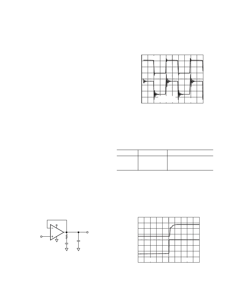
Power-Up Behavior
On power-up, the AD857x will settle to a valid output within 5
μ
s.
Figure 54a shows an oscilloscope photo of the output of the ampli-
fier along with the power supply voltage, and Figure 54b shows the
test circuit. With the amplifier configured for unity gain, the device
takes approximately 5
μ
s to settle to its final output voltage. This
turn-on response time is much faster than most other autocorrection
amplifiers, which can take hundreds of microseconds or longer for
their output to settle.
5
m
s
1V
V
OUT
V+
0V
0V
BOTTOM TRACE = 2V/DIV
TOP TRACE = 1V/DIV
Figure 54a. AD857x Output Behavior on Power-Up
相關PDF資料 |
PDF描述 |
|---|---|
| AD8582CHIPS | +5 Volt, Parallel Input Complete Dual 12-Bit DAC |
| AD8582AN | +5 Volt, Parallel Input Complete Dual 12-Bit DAC |
| AD8582AR | +5 Volt, Parallel Input Complete Dual 12-Bit DAC |
| AD8591 | CMOS Single Supply Rail-to-Rail Input/Output Operational Amplifiers with Shutdown |
| AD8591ART | CMOS Single Supply Rail-to-Rail Input/Output Operational Amplifiers with Shutdown |
相關代理商/技術參數 |
參數描述 |
|---|---|
| AD8571ARM-R2 | 制造商:Analog Devices 功能描述:SP Amp Chopper Stabilization Single R-R I/O 5V 8-Pin MSOP T/R 制造商:Rochester Electronics LLC 功能描述:DUAL PRECISION RAIL-RAIL CHOPPER OPAMP - Bulk |
| AD8571ARM-REEL | 制造商:Analog Devices 功能描述:SP Amp Chopper Stabilization Single R-R I/O 5V 8-Pin MSOP T/R 制造商:Rochester Electronics LLC 功能描述:DUAL PRECISION RAIL-RAIL CHOPPER OPAMP - Tape and Reel |
| AD8571ARMZ | 功能描述:IC OPAMP CHOPPER R-R 30MA 8MSOP RoHS:是 類別:集成電路 (IC) >> Linear - Amplifiers - Instrumentation 系列:- 標準包裝:50 系列:- 放大器類型:通用 電路數:2 輸出類型:滿擺幅 轉換速率:1.8 V/µs 增益帶寬積:6.5MHz -3db帶寬:4.5MHz 電流 - 輸入偏壓:5nA 電壓 - 輸入偏移:100µV 電流 - 電源:65µA 電流 - 輸出 / 通道:35mA 電壓 - 電源,單路/雙路(±):1.8 V ~ 5.25 V,±0.9 V ~ 2.625 V 工作溫度:-40°C ~ 85°C 安裝類型:表面貼裝 封裝/外殼:10-TFSOP,10-MSOP(0.118",3.00mm 寬) 供應商設備封裝:10-MSOP 包裝:管件 |
| AD8571ARMZ-R2 | 制造商:Analog Devices 功能描述:SP Amp Chopper Stabilization Single R-R I/O 5V 8-Pin MSOP T/R |
| AD8571ARMZ-REEL | 功能描述:IC OPAMP CHOPPER R-R 30MA 8MSOP RoHS:是 類別:集成電路 (IC) >> Linear - Amplifiers - Instrumentation 系列:- 產品培訓模塊:Differential Circuit Design Techniques for Communication Applications 標準包裝:1 系列:- 放大器類型:RF/IF 差分 電路數:1 輸出類型:差分 轉換速率:9800 V/µs 增益帶寬積:- -3db帶寬:2.9GHz 電流 - 輸入偏壓:3µA 電壓 - 輸入偏移:- 電流 - 電源:40mA 電流 - 輸出 / 通道:- 電壓 - 電源,單路/雙路(±):3 V ~ 3.6 V 工作溫度:-40°C ~ 85°C 安裝類型:表面貼裝 封裝/外殼:16-VQFN 裸露焊盤,CSP 供應商設備封裝:16-LFCSP-VQ 包裝:剪切帶 (CT) 產品目錄頁面:551 (CN2011-ZH PDF) 其它名稱:ADL5561ACPZ-R7CT |
發布緊急采購,3分鐘左右您將得到回復。