- 您現(xiàn)在的位置:買賣IC網(wǎng) > PDF目錄373951 > AD8608 (Analog Devices, Inc.) Precision Low noise CMOS Rail-to-Rail Input/Output Operational Amplifiers PDF資料下載
參數(shù)資料
| 型號: | AD8608 |
| 廠商: | Analog Devices, Inc. |
| 英文描述: | Precision Low noise CMOS Rail-to-Rail Input/Output Operational Amplifiers |
| 中文描述: | 精密低噪聲CMOS軌到軌輸入/輸出運算放大器 |
| 文件頁數(shù): | 14/20頁 |
| 文件大小: | 559K |
| 代理商: | AD8608 |
AD8605/AD8606/AD8608
Rev. D | Page 14 of 20
FREQUENCY (Hz)
0.1
0.01
0.0001
20
20k
100
T
1k
0.001
10k
V
SY
= 2.5V
A
V
= 1
B
W
= 22kHz
0
Figure 45. THD + N
TOTAL NOISE INCLUDING SOURCE RESISTORS
The low input current noise and input bias current of the
AD8605 make it the ideal amplifier for circuits with substantial
input source resistance such as photodiodes. Input offset voltage
increases by less than 0.5 nV per 1 k of source resistance at
room temperature and increases to 10 nV at 85°C. The total
noise density of the circuit is
(
)
S
n
n
TOTAL
,
S
n
TR
k
R
i
e
e
4
2
2
+
+
=
where:
e
n
is the input voltage noise density of the AD8605
i
n
is the input current noise density of the AD8605
R
S
is the source resistance at the noninverting terminal
k
is Boltzmann’s constant (1.38 × 10
23
J/K)
T
is the ambient temperature in Kelvin (T = 273 + °C)
For example, with
R
S
= 10 k, the total voltage noise density is
roughly 15 nV/√Hz.
For
R
S
< 3.9
k
, e
n
dominates and e
n,TOTAL
≈
e
n
.
The current noise of the AD8605 is so low that its total density
does not become a significant term unless R
S
is greater than
6 M. The total equivalent rms noise over a specific bandwidth
is expressed as
(
e
E
TOTAL
n
n
,
)
BW
=
where
BW
is the bandwidth in hertz.
Note that the analysis above is valid for frequencies greater than
100 Hz and assumes relatively flat noise, above 10 kHz. For
lower frequencies, flicker noise (1/f) must be considered.
CHANNEL SEPARATION
Channel separation, or inverse crosstalk, is a measure of the
signal feed from one amplifier (channel) to an other on the
same IC.
The AD8606 has a channel separation of greater than 160 dB
up to frequencies of 1 MHz, allowing the two amplifiers to
amplify ac signals independently in most applications.
C
FREQUENCY (Hz)
10M
1M
100k
10k
1k
100
100M
–20
0
–40
–60
–80
–100
–120
–140
–160
–180
0
Figure 46. Channel Separation vs. Frequency
CAPACITIVE LOAD DRIVE
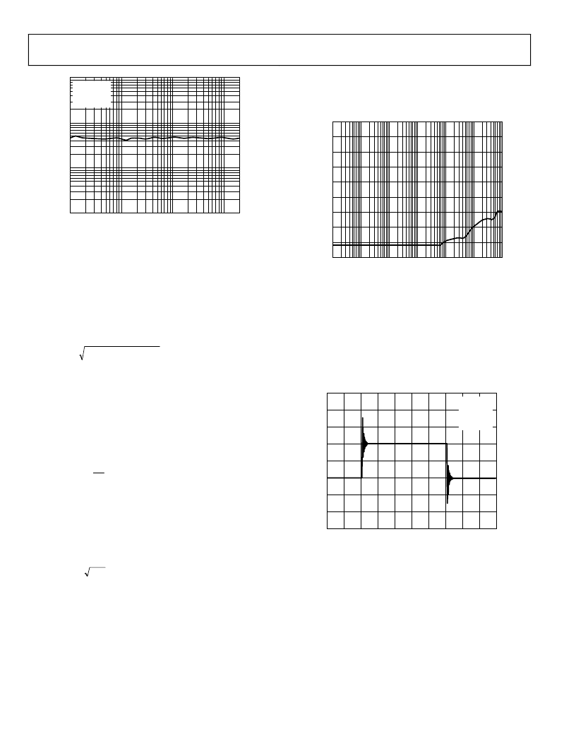
The AD8605 can drive large capacitive loads without oscillation.
Figure 47 shows the output of the AD8606 in response to a
200 mV input signal. In this case, the amplifier was configured
in positive unity gain, worst case for stability, while driving a
1,000 pF load at its output. Driving larger capacitive loads in
unity gain may require the use of additional circuitry.
TIME (10
μ
s/DIV)
V
V
S
= ±2.5V
A
V
= 1
R
L
= 10k
C
L
= 1
0
Figure 47. Capacitive Load Drive without Snubber
A snubber network, shown in Figure 48, helps reduce the signal
overshoot to a minimum and maintain stability. Although this
circuit does not recover the loss of bandwidth induced by large
capacitive loads, it greatly reduces the overshoot and ringing.
This method does not reduce the maximum output swing of
the amplifier.
Figure 49 shows a scope photograph of the output at the
snubber circuit. The overshoot is reduced from over 70% to
less than 5%, and the ringing is eliminated by the snubber.
Optimum values for R
S
and C
S
are determined experimentally.
相關(guān)PDF資料 |
PDF描述 |
|---|---|
| AD8608AR | Precision Low noise CMOS Rail-to-Rail Input/Output Operational Amplifiers |
| AD8608ARU | Precision Low noise CMOS Rail-to-Rail Input/Output Operational Amplifiers |
| AD8605ART-REEL | Precision Low noise CMOS Rail-to-Rail Input/Output Operational Amplifiers |
| AD8605ART-REEL7 | Precision Low noise CMOS Rail-to-Rail Input/Output Operational Amplifiers |
| AD8605ARTZ-REEL | Precision Low noise CMOS Rail-to-Rail Input/Output Operational Amplifiers |
相關(guān)代理商/技術(shù)參數(shù) |
參數(shù)描述 |
|---|---|
| AD8608_CN | 制造商:AD 制造商全稱:Analog Devices 功能描述:精密、低噪聲、CMOS軌到軌輸入/輸出運算放大器 |
| AD8608AR | 制造商:Analog Devices 功能描述:IC OP-AMP QUAD R/R |
| AD8608ARN | 制造商:未知廠家 制造商全稱:未知廠家 功能描述:Operational Amplifier |
| AD8608AR-REEL | 制造商:Analog Devices 功能描述:OP Amp Quad GP R-R I/O 5.5V 14-Pin SOIC N T/R |
| AD8608AR-REEL7 | 制造商:Analog Devices 功能描述:OP Amp Quad GP R-R I/O 5.5V 14-Pin SOIC N T/R |
發(fā)布緊急采購,3分鐘左右您將得到回復(fù)。