- 您現(xiàn)在的位置:買賣IC網(wǎng) > PDF目錄373959 > AD9101SE (ANALOG DEVICES INC) 125 MSPS Monolithic Sampling Amplifier PDF資料下載
參數(shù)資料
| 型號: | AD9101SE |
| 廠商: | ANALOG DEVICES INC |
| 元件分類: | 運(yùn)動控制電子 |
| 英文描述: | 125 MSPS Monolithic Sampling Amplifier |
| 中文描述: | TRACK AND HOLD AMPLIFIER, CQCC20 |
| 封裝: | CERAMIC, LCC-20 |
| 文件頁數(shù): | 5/12頁 |
| 文件大小: | 247K |
| 代理商: | AD9101SE |
AD9101
–5–
REV. 0
V
OUT
TS
ACQUISITION TIME
AT HC TO X%
V
OUT
TRACK
HOLD
TRACK-TO-HOLD
INDUCED GLITCH
V
HC
t
DHT
1.5ns
V
HC
AMP
HC
SAMPLER
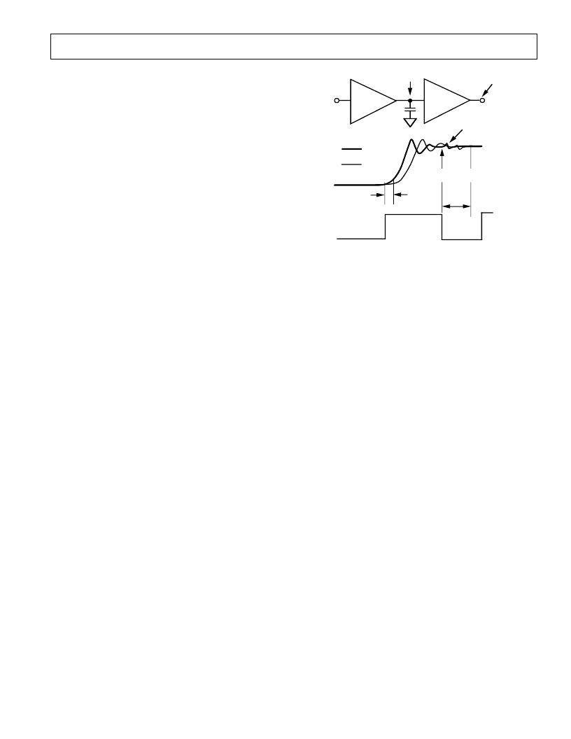
Figure 1. Acquisition Time at Hold Capacitor
during the track time. However, since the output amplifier al-
ways “tracks” the front end circuitry, it “catches up” and di-
rectly superimposes itself (less about 500 ps of analog delay) to
V
HC
. Since the small signal settling time of the output amplifier
can be about 1.2 ns to
±
1 mV, and is significantly less than the
hold time, acquisition time should be referenced to the hold
capacitor.
Most of the hold settling time and output acquisition time are
due to the sampler and the switch network. (Output acquisition
time is as seen on a scope at the output. T his is typically 1.7 ns
longer than actual acquisition time.) For track time, the output
amplifier contributes only about 5 ns of the total; in hold mode,
it contributes 1.7 ns (as stated above).
A stricter definition of acquisition would actually include both
the acquisition and track-to-hold settling times to a defined ac-
curacy. T o obtain 12-bit+ distortion levels and 50 MSPS opera-
tion, the minimum recommended track and hold times are
12 ns and 8 ns, respectively. T o drive an 8-bit flash converter
(such as the AD9002) with a 2 V p-p full-scale input, hold time
to 1 LSB accuracy will be limited primarily by the aperture time
of the encoder, rather than by the AD9101. T his makes it pos-
sible to reduce track time to as little as 5 ns, with hold time cho-
sen to optimize the encoder’s performance.
T hough acquisition time and track-to-hold settling time to
1/2 LSB (0.4%) accuracy are 6 ns and 4 ns respectively, it is still
possible to achieve –45 dB SNR performance at clock speeds to
125 MSPS. T his is because the settling error is roughly propor-
tional to the signal level and is partially cancelled due to the
high phase margin of the input sampler.
Hold vs. T rack Mode Distortion
In many traditional high speed, open-loop track-and-holds,
track mode distortion is often much better than hold mode dis-
tortion. T rack mode distortion does not include nonlinearities
due to the switch network, and does not correlate to the relevant
hold mode distortion. But since hold mode distortion has tradi-
tionally been omitted from manufacturer’s specification tables,
users have had to discover for themselves the effective overall
hold mode distortion of the combined T /H and encoder.
T HE ORY OF OPE RAT ION
T he AD9101 employs a new and unique track-and-hold archi-
tecture. Previous commercially available high speed track-and-
holds used an open loop input buffer, followed by a diode
bridge, hold capacitor, and output buffer (closed or open loop)
with a FET device usually connected to the hold capacitor. T his
architecture required mixed device technology and, usually, hy-
brid construction. T he sampling rate of these hybrids has been
limited to 20 MSPS for 12-bit accuracy. Distortion generated in
the front-end amplifier/bridge limited the dynamic range perfor-
mance to the “mid –70 dBFS” for analog input signals of less
than 10 MHz. Broadband and switch-generated noise limited
the SNR of previous track-and-holds to about 70 dB.
T he AD9101 is a monolithic device using a high frequency
complementary bipolar process to achieve new levels of high
speed precision. Its architecture completely breaks from the tra-
ditional architecture described above. T he hold switch has been
integrated into the first stage closed-loop buffer. T his innova-
tion provides error (distortion) correction for both the switch
and buffer while still achieving slew rates representative of an
open-loop design. In addition, acquisition slew current for the
hold capacitor is higher than the traditional diode bridge switch
configurations, removing a main contributor to the limits of
maximum sampling rate, input frequency, and distortion.
T he closed-loop output amplifier includes zero voltage bias cur-
rent cancellation, which results in high-temperature droop rates
close to those found in FET type inputs. T his closed-loop am-
plifier inherently provides high speed loop correction and has
extremely low distortion even when heavily loaded.
Extremely fast time constant linearity (7 ns to 0.01% for a 4 V
output step) ensures that the output amplifier does not limit the
AD9101 sampling rate or analog input frequency. (T he acquisi-
tion and settling time are primarily limited only by the input
sampler.) T he output is transparent to the overall AD9101 hold
mode distortion levels for loads as low as 50
.
Full-scale track and acquisition slew rates achieved by the
AD9101 are 1800 V/
μ
s and 1700 V/
μ
s, respectively. When com-
bined with excellent phase margin (typically 5% overshoot),
wide bandwidth, and dc gain accuracy, acquisition time to
0.01% is only 11 ns.
Acquisition T ime
Acquisition time is the amount of time it takes the AD9101 to
reacquire the analog input when switching from hold-to-track
mode. T he interval starts at the 50% clock transition point and
ends when the input signal is reacquired to within a specified er-
ror band at the hold capacitor.
T he hold-to-track switch delay (t
DHT
) cannot be subtracted
from this acquisition time for 12-bit performance because it is a
charging time and analog output delay that occurs when moving
from hold to track; this delay is typically 1.5 ns. T herefore, the
track time required for the AD9101 is the acquisition time
which includes t
DHT
. Note that the acquisition time is defined as
the settled voltage at the hold capacitor and does not include the
delay and settling time of the output amplifier. T he example in
Figure 1 illustrates why the output amplifier does not contribute
to the overall acquisition time.
T he exaggerated illustration in Figure 1 shows that V
HC
has
settled to within x% of its final value, but V
OUT
(due to slew rate
limitations, finite BW, power supply ringing, etc.) has not settled
相關(guān)PDF資料 |
PDF描述 |
|---|---|
| AD9101 | 125 MSPS Monolithic Sampling Amplifier(125MSPS單片采樣放大器) |
| AD9200KST | Complete 10-Bit, 20 MSPS, 80 mW CMOS A/D Converter |
| AD9200LQFP-EVAL | Complete 10-Bit, 20 MSPS, 80 mW CMOS A/D Converter |
| AD9200JRSRL | Complete 10-Bit, 20 MSPS, 80 mW CMOS A/D Converter |
| AD9200ARSRL | Complete 10-Bit, 20 MSPS, 80 mW CMOS A/D Converter |
相關(guān)代理商/技術(shù)參數(shù) |
參數(shù)描述 |
|---|---|
| AD9102 | 制造商:AD 制造商全稱:Analog Devices 功能描述:Low Power, 14-Bit, 180 MSPS, Digital-to-Analog Converter and Waveform Generator |
| AD91020 | 制造商:Analog Devices 功能描述: |
| AD9102BCPZ | 功能描述:數(shù)模轉(zhuǎn)換器- DAC 14 bit Single Channel DAC RoHS:否 制造商:Texas Instruments 轉(zhuǎn)換器數(shù)量:1 DAC 輸出端數(shù)量:1 轉(zhuǎn)換速率:2 MSPs 分辨率:16 bit 接口類型:QSPI, SPI, Serial (3-Wire, Microwire) 穩(wěn)定時間:1 us 最大工作溫度:+ 85 C 安裝風(fēng)格:SMD/SMT 封裝 / 箱體:SOIC-14 封裝:Tube |
| AD9102BCPZRL7 | 功能描述:數(shù)模轉(zhuǎn)換器- DAC Low Power 14-Bit 180MSPS RoHS:否 制造商:Analog Devices 轉(zhuǎn)換器數(shù)量:4 DAC 輸出端數(shù)量:4 轉(zhuǎn)換速率: 分辨率:12 bit 接口類型:Serial (I2C) 穩(wěn)定時間: 最大工作溫度:+ 105 C 安裝風(fēng)格: 封裝 / 箱體:TSSOP 封裝:Reel |
| AD9102-EBZ | 功能描述:數(shù)據(jù)轉(zhuǎn)換 IC 開發(fā)工具 14 bit Single Channel DAC RoHS:否 制造商:Texas Instruments 產(chǎn)品:Demonstration Kits 類型:ADC 工具用于評估:ADS130E08 接口類型:SPI 工作電源電壓:- 6 V to + 6 V |
發(fā)布緊急采購,3分鐘左右您將得到回復(fù)。