- 您現在的位置:買賣IC網 > PDF目錄373959 > AD9200LQFP-EVAL (Analog Devices, Inc.) Complete 10-Bit, 20 MSPS, 80 mW CMOS A/D Converter PDF資料下載
參數資料
| 型號: | AD9200LQFP-EVAL |
| 廠商: | Analog Devices, Inc. |
| 英文描述: | Complete 10-Bit, 20 MSPS, 80 mW CMOS A/D Converter |
| 中文描述: | 完整的10位,20 MSPS的80毫瓦的CMOS A / D轉換 |
| 文件頁數: | 15/24頁 |
| 文件大小: | 338K |
| 代理商: | AD9200LQFP-EVAL |
AD9200
–15–
REV. E
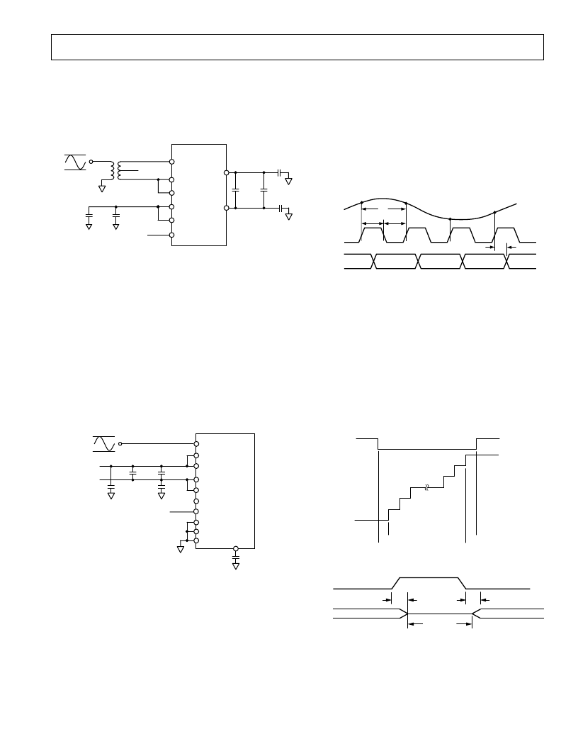
DIFFERENTIAL INPUT OPERATION
The AD9200 will accept differential input signals. This function
may be used by shorting REFTS and REFBS and driving them
as one leg of the differential signal (the top leg is driven into
AIN). In the configuration below, the AD9200 is accepting a
1 V p-p signal. See Figure 29.
AIN
REFTS
REFTF
REFBF
REFBS
AD9200
0.1
m
F
10
m
F
0.1
m
F
0.1
m
F
2V
1V
AVDD/2
VREF
REFSENSE
MODE
AVDD/2
0.1
m
F
1.0
m
F
Figure 29. Differential Input
AD876 MODE OF OPERATION
The AD9200 may be dropped into the AD876 socket. This will
allow AD876 users to take advantage of the reduced power
consumption realized when running the AD9200 on a 3.0 V
analog supply.
Figure 30 shows the pin functions of the AD876 and AD9200.
The grounded REFSENSE pin and floating MODE pin effec-
tively put the AD9200 in the external reference mode. The
external reference input for the AD876 will now be placed on
the reference pins of the AD9200.
The clamp controls will be grounded by the AD876 socket. The
AD9200 has a 3 clock cycle delay compared to a 3.5 cycle delay
of the AD876.
4V
2V
0.1
m
F
0.1
m
F
AVDD
10
m
F
0.1
m
F
4V
2V
AIN
REFTS
REFTF
REFBF
REFBS
CLAMP
CLAMPIN
OTR
REFSENSE
AD9200
MODE
NC
VREF
0.1
m
F
Figure 30. AD876 Mode
CLOCK INPUT
The AD9200 clock input is buffered internally with an inverter
powered from the AVDD pin. This feature allows the AD9200
to accommodate either +5 V or +3.3 V CMOS logic input sig-
nal swings with the input threshold for the CLK pin nominally
at AVDD/2.
The pipelined architecture of the AD9200 operates on both
rising and falling edges of the input clock. To minimize duty
cycle variations the recommended logic family to drive the clock
input is high speed or advanced CMOS (HC/HCT, AC/ACT)
logic. CMOS logic provides both symmetrical voltage threshold
levels and sufficient rise and fall times to support 20 MSPS
operation. The AD9200 is designed to support a conversion rate
of 20 MSPS; running the part at slightly faster clock rates may
be possible, although at reduced performance levels. Conversely,
some slight performance improvements might be realized by
clocking the AD9200 at slower clock rates.
t
CL
t
CH
t
C
25ns
DATA 1
DATA
OUTPUT
INPUT
CLOCK
ANALOG
INPUT
S1
S2
S3
S4
Figure 31. Timing Diagram
The power dissipated by the output buffers is largely propor-
tional to the clock frequency; running at reduced clock rates
provides a reduction in power consumption.
DIGITAL INPUTS AND OUTPUTS
Each of the AD9200 digital control inputs, THREE-STATE
and STBY are reference to analog ground. The clock is also
referenced to analog ground.
The format of the digital output is straight binary (see Figure
32). A low power mode feature is provided such that for STBY
= HIGH and the clock disabled, the static power of the AD9200
will drop below 5 mW.
OTR
–FS
–FS+1LSB
+FS–1LSB
+FS
Figure 32. Output Data Format
HIGH
IMPEDANCE
t
DHZ
t
DEN
THREE-
STATE
DATA
(D0–D9)
Figure 33. Three-State Timing Diagram
相關PDF資料 |
PDF描述 |
|---|---|
| AD9200JRSRL | Complete 10-Bit, 20 MSPS, 80 mW CMOS A/D Converter |
| AD9200ARSRL | Complete 10-Bit, 20 MSPS, 80 mW CMOS A/D Converter |
| AD9200 | Complete 10-Bit, 20 MSPS, 80 mW CMOS A/D Converter |
| AD9200ARS | CAP 33 UF 16V 10% |
| AD9200JRS | Complete 10-Bit, 20 MSPS, 80 mW CMOS A/D Converter |
相關代理商/技術參數 |
參數描述 |
|---|---|
| AD9200SSOP-EVAL | 制造商:Analog Devices 功能描述:Evaluation Board For AD9200 CMOS A/D Converter 制造商:Analog Devices 功能描述:EVAL BD FOR AD9200 CMOS A/D CNVRTR - Bulk |
| AD9200TQFP-EVAL | 制造商:Analog Devices 功能描述:EVAL BD FOR AD9200 CMOS A/D CNVRTR - Bulk |
| AD9201 | 制造商:AD 制造商全稱:Analog Devices 功能描述:Dual Channel, 20 MHz 10-Bit Resolution CMOS ADC |
| AD9201ARS | 功能描述:IC ADC CMOS 10BIT DUAL 28-SSOP RoHS:否 類別:集成電路 (IC) >> 數據采集 - 模數轉換器 系列:- 標準包裝:1,000 系列:- 位數:12 采樣率(每秒):300k 數據接口:并聯 轉換器數目:1 功率耗散(最大):75mW 電壓電源:單電源 工作溫度:0°C ~ 70°C 安裝類型:表面貼裝 封裝/外殼:24-SOIC(0.295",7.50mm 寬) 供應商設備封裝:24-SOIC 包裝:帶卷 (TR) 輸入數目和類型:1 個單端,單極;1 個單端,雙極 |
| AD9201ARSRL | 功能描述:IC ADC 10BIT 2CH 40MSPS 28-SSOP RoHS:否 類別:集成電路 (IC) >> 數據采集 - 模數轉換器 系列:- 標準包裝:1,000 系列:- 位數:16 采樣率(每秒):45k 數據接口:串行 轉換器數目:2 功率耗散(最大):315mW 電壓電源:模擬和數字 工作溫度:0°C ~ 70°C 安裝類型:表面貼裝 封裝/外殼:28-SOIC(0.295",7.50mm 寬) 供應商設備封裝:28-SOIC W 包裝:帶卷 (TR) 輸入數目和類型:2 個單端,單極 |
發布緊急采購,3分鐘左右您將得到回復。