- 您現在的位置:買賣IC網 > PDF目錄373959 > AD9201-EVAL (Analog Devices, Inc.) Dual Channel, 20 MHz 10-Bit Resolution CMOS ADC PDF資料下載
參數資料
| 型號: | AD9201-EVAL |
| 廠商: | Analog Devices, Inc. |
| 英文描述: | Dual Channel, 20 MHz 10-Bit Resolution CMOS ADC |
| 中文描述: | 雙通道,20 MHz的10位分辨率的CMOS模數轉換器 |
| 文件頁數: | 9/20頁 |
| 文件大小: | 431K |
| 代理商: | AD9201-EVAL |
AD9201
–9–
REV. D
The AD9201 can accommodate a variety of input spans be-
tween 1 V and 2 V. For spans of less than 1 V, expect a propor-
tionate degradation in SNR . Use of a 2 V span will provide the
best noise performance. 1 V spans will provide lower distortion
when using a 3 V analog supply. Users wishing to run with
larger full-scales are encouraged to use a 5 V analog supply
(AVDD).
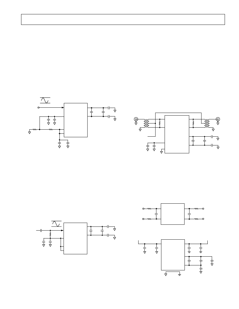
Single-Ended Inputs:
For single-ended input signals, the
signal is applied to one input pin and the other input pin is tied
to a midscale voltage. This midscale voltage defines the center
of the full-scale span for the input signal.
EXAMPLE: For a single-ended input range from 0 V to 1 V
applied to IINA, we would configure the converter for a 1 V
reference (See Figure 17) and apply 0.5 V to IINB.
I OR QREFT
I OR QREFB
IINA
IINB
VREF
REFSENSE
0.1
m
F
10
m
F
0.1
m
F
0.1
m
F
0.1
m
F
AD9201
0.1
m
F
10
m
F
10
m
F
MIDSCALE
VOLTAGE
= 0.5V
1V
0V
INPUT
5k
V
5k
V
Figure 17. Example Configuration for 0 V–1 V Single-
Ended Input Signal
Note that since the inputs are high impedance, this reference
level can easily be generated with an external resistive divider
with large resistance values (to minimize power dissipation). A
decoupling capacitor is recommended on this input to minimize
the high frequency noise-coupling onto this pin. Decoupling
should occur close to the ADC.
Differential Inputs
Use of differential input signals can provide greater flexibility in
input ranges and bias points, as well as offering improvements in
distortion performance, particularly for high frequency input
signals. Users with differential input signals will probably want
to take advantage of the differential input structure.
0.1
m
F
10
m
F
0.1
m
F
0.1
m
F
ANALOG
INPUT
C1
C2
1.0
m
F
C3
0.1
m
F
R1
1k
V
1.5V
0.5V
REFT
REFB
IINA
IINB
VREF
AD9201
REFSENSE
Figure 18. Example Configuration for 0.5 V–1.5 V ac
Coupled Single-Ended Inputs
AC Coupled Inputs
If the signal of interest has no dc component, ac coupling can be
easily used to define an optimum bias point. Figure 18 illus-
trates one recommended configuration. The voltage chosen for
the dc bias point (in this case the 1 V reference) is applied to
both IINA and IINB pins through 1 k
resistors (R1 and R2).
IINA is coupled to the input signal through Capacitor C1, while
IINB is decoupled to ground through Capacitor C2 and C3.
Transformer Coupled Inputs
Another option for input ac coupling is to use a transformer.
This not only provides dc rejection, but also allows truly differ-
ential drive of the AD9201’s analog inputs, which will provide
the optimal distortion performance. Figure 19 shows a recom-
mended transformer input drive configuration. Resistors R1 and
R2 define the termination impedance of the transformer coupling.
The center tap of the transformer secondary is tied to the com-
mon-mode reference, establishing the dc bias point for the ana-
log inputs.
0.1
m
F
10
m
F
0.1
m
F
0.1
m
F
COMMON
MODE
VOLTAGE
0.1
m
F
10
m
F
R1
R2
I OR QREFT
I OR QREFB
IINA
IINB
AD9201
QINB
QINA
REFSENSE
VREF
Figure 19. Example Configuration for Transformer
Coupled Inputs
Crosstalk:
The internal layout of the AD9201, as well as its
pinout, was configured to minimize the crosstalk between the
two input signals. Users wishing to minimize high frequency
crosstalk should take care to provide the best possible decoupling
for input pins (see Figure 20). R and C values will make a pole
dependant on antialiasing requirements. Decoupling is also
required on reference pins and power supplies (see Figure 21).
QINA
QINB
IINA
IINB
AD9201
Figure 20. Input Loading
DVDD
I OR QREFT
I OR QREFB
AVDD
0.1
m
F
10
m
F
0.1
m
F
10
m
F
AD9201
0.1
m
F
0.1
m
F
0.1
m
F
10
m
F
V ANALOG
V DIGITAL
Figure 21. Reference and Power Supply Decoupling
相關PDF資料 |
PDF描述 |
|---|---|
| AD9201ARS | Dual Channel, 20 MHz 10-Bit Resolution CMOS ADC |
| AD9201EVALBOARD | Octal I2C 16-Bit Rail-to-Rail DACs in 16-Lead SSOP; Package: SSOP; No of Pins: 16; Temperature Range: -40°C to +85°C |
| AD9203 | 10-Bit, 40 MSPS, 3 V, 74 mW A/D Converter |
| AD9203-EB | 10-Bit, 40 MSPS, 3 V, 74 mW A/D Converter |
| AD9203ARU | 10-Bit, 40 MSPS, 3 V, 74 mW A/D Converter |
相關代理商/技術參數 |
參數描述 |
|---|---|
| AD9201EVALBOARD | 制造商:AD 制造商全稱:Analog Devices 功能描述:*AD9201 EVAL BOARD* |
| AD9202JRS | 制造商:Analog Devices 功能描述: |
| AD9202JRSRL | 制造商:未知廠家 制造商全稱:未知廠家 功能描述:Analog-to-Digital Converter, 10-Bit |
| AD9203 | 制造商:AD 制造商全稱:Analog Devices 功能描述:10-Bit, 40 MSPS, 3 V, 74 mW A/D Converter |
| AD9203ARU | 功能描述:IC ADC 10BIT 40MSPS 3V 28-TSSOP RoHS:否 類別:集成電路 (IC) >> 數據采集 - 模數轉換器 系列:- 標準包裝:1,000 系列:- 位數:16 采樣率(每秒):45k 數據接口:串行 轉換器數目:2 功率耗散(最大):315mW 電壓電源:模擬和數字 工作溫度:0°C ~ 70°C 安裝類型:表面貼裝 封裝/外殼:28-SOIC(0.295",7.50mm 寬) 供應商設備封裝:28-SOIC W 包裝:帶卷 (TR) 輸入數目和類型:2 個單端,單極 |
發布緊急采購,3分鐘左右您將得到回復。