- 您現在的位置:買賣IC網 > PDF目錄373959 > AD9201EVALBOARD (Analog Devices, Inc.) Octal I2C 16-Bit Rail-to-Rail DACs in 16-Lead SSOP; Package: SSOP; No of Pins: 16; Temperature Range: -40°C to +85°C PDF資料下載
參數資料
| 型號: | AD9201EVALBOARD |
| 廠商: | Analog Devices, Inc. |
| 英文描述: | Octal I2C 16-Bit Rail-to-Rail DACs in 16-Lead SSOP; Package: SSOP; No of Pins: 16; Temperature Range: -40°C to +85°C |
| 中文描述: | * AD9201 EVAL委員會* |
| 文件頁數: | 13/20頁 |
| 文件大小: | 431K |
| 代理商: | AD9201EVALBOARD |
AD9201
–13–
REV. D
DIGITAL INPUTS AND OUTPUTS
Each of the AD9201 digital control inputs, CHIP SELECT,
CLOCK, SELECT and SLEEP are referenced to AVDD and
AVSS. Switching thresholds will be AVDD/2.
The format of the digital output is straight binary. A low power
mode feature is provided such that for STBY = HIGH and the
clock disabled, the static power of the AD9201 will drop below
22 mW.
CLOCK INPUT
The AD9201 clock input is internally buffered with an inverter
powered from the AVDD pin. This feature allows the AD9201
to accommodate either +5 V or +3.3 V CMOS logic input sig-
nal swings with the input threshold for the CLK pin nominally
at AVDD/2.
The pipelined architecture of the AD9201 operates on both
rising and falling edges of the input clock. To minimize duty
cycle variations the logic family recommended to drive the clock
input is high speed or advanced CMOS (HC/HCT, AC/ACT)
logic. CMOS logic provides both symmetrical voltage threshold
levels and sufficient rise and fall times to support 20 MSPS
operation. Running the part at slightly faster clock rates may be
possible, although at reduced performance levels. Conversely,
some slight performance improvements might be realized by
clocking the AD9201 at slower clock rates.
The power dissipated by the output buffers is largely propor-
tional to the clock frequency; running at reduced clock rates
provides a reduction in power consumption.
DIGITAL OUTPUTS
Each of the on-chip buffers for the AD9201 output bits (D0–D9)
is powered from the DVDD supply pin, separate from AVDD.
The output drivers are sized to handle a variety of logic families
while minimizing the amount of glitch energy generated. In all
cases, a fan-out of one is recommended to keep the capacitive
load on the output data bits below the specified 20 pF level.
For DVDD = 5 V, the AD9201 output signal swing is compat-
ible with both high speed CMOS and TTL logic families. For
TTL, the AD9201 on-chip, output drivers were designed to
support several of the high speed TTL families (F, AS, S). For
applications where the clock rate is below 20 MSPS, other TTL
families may be appropriate. For interfacing with lower voltage
CMOS logic, the AD9201 sustains 20 MSPS operation with
DVDD = 3 V. In all cases, check your logic family data sheets
for compatibility with the AD9201’s Specification table.
A 2 ns reduction in output delays can be achieved by limiting
the logic load to 5 pF per output line.
THREE-STATE OUTPUTS
The digital outputs of the AD9201 can be placed in a high
impedance state by setting the CHIP SELECT pin to HIGH.
This feature is provided to facilitate in-circuit testing or evaluation.
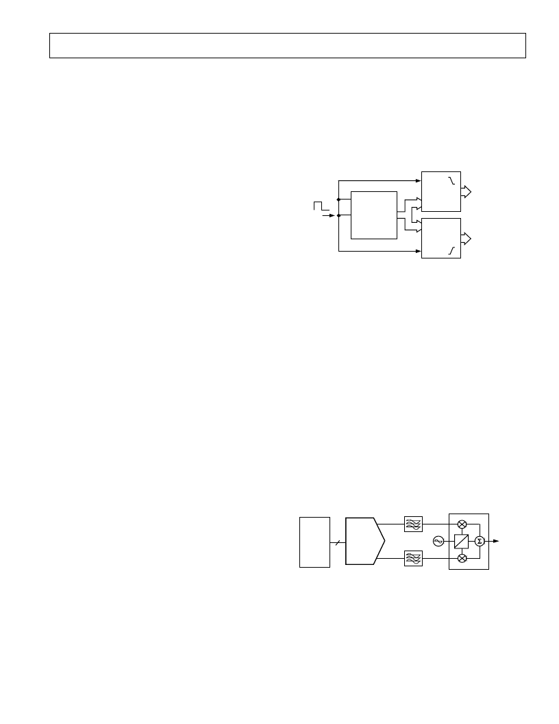
SELECT
When the select pin is held LOW, the output word will present
the “Q” level. When the select pin is held HIGH, the “I” level
will be presented to the output word (see Figure 1).
The AD9201’s select and clock pins may be driven by a com-
mon signal source. The data will change in 5 ns to 11 ns after
the edges of the input pulse. The user must make sure the inter-
face latches have sufficient hold time for the AD9201’s delays
(see Figure 30).
CLOCK
DATA
I LATCH
CLOCK
DATA
Q LATCH
CLK
DATA
OUT
SELECT
I
PROCESSING
Q
PROCESSING
CLOCK
SOURCE
Figure 30. Typical De-Mux Connection
APPLICATIONS
USING THE AD9201 FOR QAM DEMODULATION
QAM is one of the most widely used digital modulation schemes
in digital communication systems. This modulation technique
can be found in both FDMA as well as spread spectrum (i.e.,
CDMA) based systems. A QAM signal is a carrier frequency
which is both modulated in amplitude (i.e., AM modulation)
and in phase (i.e., PM modulation). At the transmitter, it can
be generated by independently modulating two carriers of iden-
tical frequency but with a 90
°
phase difference. This results in
an inphase (I) carrier component and a quadrature (Q) carrier
component at a 90
°
phase shift with respect to the I component.
The I and Q components are then summed to provide a QAM
signal at the specified carrier or IF frequency. Figure 31 shows
a typical analog implementation of a QAM modulator using a
dual 10-bit DAC with 2
×
interpolation, the AD9761. A QAM
signal can also be synthesized in the digital domain thus requir-
ing a single DAC to reconstruct the QAM signal. The AD9853
is an example of a complete (i.e., DAC included) digital QAM
modulator.
0
90
DSP
OR
ASIC
10
CARRIER
FREQUENCY
NYQUIST
FILTERS
TO
MIXER
QUADRATURE
MODULATOR
AD9761
IOUT
QOUT
Figure 31. Typical Analog QAM Modulator Architecture
相關PDF資料 |
PDF描述 |
|---|---|
| AD9203 | 10-Bit, 40 MSPS, 3 V, 74 mW A/D Converter |
| AD9203-EB | 10-Bit, 40 MSPS, 3 V, 74 mW A/D Converter |
| AD9203ARU | 10-Bit, 40 MSPS, 3 V, 74 mW A/D Converter |
| AD9211_07 | 10-Bit, 200 MSPS/250 MSPS/300 MSPS, 1.8 V Analog-to-Digital Converter |
| AD9211-200EBZ | 10-Bit, 200 MSPS/250 MSPS/300 MSPS, 1.8 V Analog-to-Digital Converter |
相關代理商/技術參數 |
參數描述 |
|---|---|
| AD9202JRS | 制造商:Analog Devices 功能描述: |
| AD9202JRSRL | 制造商:未知廠家 制造商全稱:未知廠家 功能描述:Analog-to-Digital Converter, 10-Bit |
| AD9203 | 制造商:AD 制造商全稱:Analog Devices 功能描述:10-Bit, 40 MSPS, 3 V, 74 mW A/D Converter |
| AD9203ARU | 功能描述:IC ADC 10BIT 40MSPS 3V 28-TSSOP RoHS:否 類別:集成電路 (IC) >> 數據采集 - 模數轉換器 系列:- 標準包裝:1,000 系列:- 位數:16 采樣率(每秒):45k 數據接口:串行 轉換器數目:2 功率耗散(最大):315mW 電壓電源:模擬和數字 工作溫度:0°C ~ 70°C 安裝類型:表面貼裝 封裝/外殼:28-SOIC(0.295",7.50mm 寬) 供應商設備封裝:28-SOIC W 包裝:帶卷 (TR) 輸入數目和類型:2 個單端,單極 |
| AD9203ARURL7 | 功能描述:IC ADC 10BIT 40MSPS 3V 28-TSSOP RoHS:否 類別:集成電路 (IC) >> 數據采集 - 模數轉換器 系列:- 標準包裝:1,000 系列:- 位數:16 采樣率(每秒):45k 數據接口:串行 轉換器數目:2 功率耗散(最大):315mW 電壓電源:模擬和數字 工作溫度:0°C ~ 70°C 安裝類型:表面貼裝 封裝/外殼:28-SOIC(0.295",7.50mm 寬) 供應商設備封裝:28-SOIC W 包裝:帶卷 (TR) 輸入數目和類型:2 個單端,單極 |
發布緊急采購,3分鐘左右您將得到回復。