- 您現在的位置:買賣IC網 > PDF目錄373959 > AD9211BCPZ-300 (ANALOG DEVICES INC) 10-Bit, 200 MSPS/250 MSPS/300 MSPS, 1.8 V Analog-to-Digital Converter PDF資料下載
參數資料
| 型號: | AD9211BCPZ-300 |
| 廠商: | ANALOG DEVICES INC |
| 元件分類: | ADC |
| 英文描述: | 10-Bit, 200 MSPS/250 MSPS/300 MSPS, 1.8 V Analog-to-Digital Converter |
| 中文描述: | 1-CH 10-BIT PROPRIETARY METHOD ADC, PARALLEL ACCESS, QCC56 |
| 封裝: | 8 X 8 MM, ROHS COMPLIANT, MO-220VLLD-2, LFCSP-56 |
| 文件頁數: | 11/28頁 |
| 文件大小: | 1180K |
| 代理商: | AD9211BCPZ-300 |
第1頁第2頁第3頁第4頁第5頁第6頁第7頁第8頁第9頁第10頁當前第11頁第12頁第13頁第14頁第15頁第16頁第17頁第18頁第19頁第20頁第21頁第22頁第23頁第24頁第25頁第26頁第27頁第28頁
AD9211
Rev. 0 | Page 11 of 28
DNC = DO NOT CONNECT
PIN 1
1
2
3
4
5
6
7
8
9
D2/D7–
D2/D7+
D3/D8–
D3/D8+
(MSB) D4/D9–
(MSB) D4/D9+
DRVDD
DRGND
OR–
OR+
DNC
DNC
DNC
DNC
10
11
12
13
14
35 VIN+
34 AVDD
33 AVDD
32 AVDD
31 RBIAS
30 AVDD
29 PWDN
36 VIN–
37 AVDD
38 AVDD
39 AVDD
40 CML
41 AVDD
42 AVDD
1
D
1
D
1
D
1
D
2
D
2
D
2
D
2
D
2
D
2
S
2
S
2
C
2
R
1
D
4
4
4
4
4
5
5
5
5
5
4
4
TOP VIEW
(Not to Scale)
PIN 0 (EXPOSED PADDLE) = AGND
AD9211
5
5
0
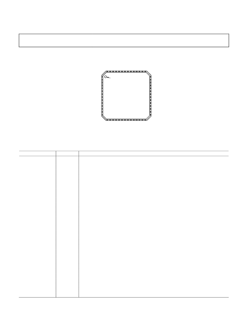
Figure 5. AD9211 Double Data Rate Pin Configuration
Table 8. Double Data Rate Mode Pin Function Descriptions
Pin No.
Mnemonic
30, 32 to 34, 37 to 39,
41 to 43, 46
7, 24, 47
DRVDD
0
AGND
1
8, 23, 48
DRGND
1
35
VIN+
36
VIN
40
CML
Description
1.8 V Analog Supply.
AVDD
1.8 V Digital Output Supply.
Analog Ground.
Digital Output Ground.
Analog Input—True.
Analog Input—Complement.
Common-Mode Output Pin. Enabled through the SPI, this pin provides a reference for the
optimized internal bias voltage for VIN+/VIN.
Clock Input—True.
Clock Input—Complement.
Set Pin for Chip Bias Current. (Place 1% 10 kΩ resistor terminated to ground.) Nominally 0.5 V.
CMOS-Compatible Chip Reset (Active Low).
Serial Port Interface (SPI) Data Input/Output (Serial Port Mode); Duty Cycle Stabilizer Select
(External Pin Mode).
Serial Port Interface Clock (Serial Port Mode); Data Format Select Pin (External Pin Mode).
Serial Port Chip Select (Active Low).
Chip Power-Down.
Data Clock Output—Complement.
Data Clock Output—True.
D1/D7 Complement Output Bit (LSB).
D1/D7 True Output Bit (LSB).
D2/D8 Complement Output Bit.
D2/D8 True Output Bit.
D3/D9 Complement Output Bit.
D3/D9 True Output Bit.
D4/D10 Complement Output Bit.
D4/D10 True Output Bit.
D5/D11 Complement Output Bit (MSB).
D5/D11 True Output Bit (MSB).
44
45
31
28
25
CLK+
CLK
RBIAS
RESET
SDIO/DCS
26
27
29
49
50
53
54
55
56
1
2
3
4
5
6
SCLK/DFS
CSB
PWDN
DCO
DCO+
D0/D5
D0/D5+
D1/D6
D1/D6+
D2/D7
D2/D7+
D3/D8
D3/D8+
D4/D9
D4/D9+
相關PDF資料 |
PDF描述 |
|---|---|
| AD9211 | 10-Bit, 170/200/250 MSPS 1.8 V A/D Converter |
| AD9211-170EB | 10-Bit, 170/200/250 MSPS 1.8 V A/D Converter |
| AD9211-200EB | 10-Bit, 170/200/250 MSPS 1.8 V A/D Converter |
| AD9211-250EB | 10-Bit, 170/200/250 MSPS 1.8 V A/D Converter |
| AD9211BCPZ-170 | 10-Bit, 170/200/250 MSPS 1.8 V A/D Converter |
相關代理商/技術參數 |
參數描述 |
|---|---|
| AD9212 | 制造商:AD 制造商全稱:Analog Devices 功能描述:Octal, 10-Bit, 40/65 MSPS Serial LVDS 1.8 V A/D Converter |
| AD9212_11 | 制造商:AD 制造商全稱:Analog Devices 功能描述:Octal, 10-Bit, 40 MSPS/65 MSPS, Serial LVDS, 1.8 V ADC |
| AD9212-65EB1 | 制造商:AD 制造商全稱:Analog Devices 功能描述:High Speed ADC USB FIFO Evaluation Kit |
| AD9212-65EBZ | 功能描述:BOARD EVALUATION FOR AD9212 RoHS:是 類別:編程器,開發系統 >> 評估板 - 模數轉換器 (ADC) 系列:- 產品培訓模塊:Obsolescence Mitigation Program 標準包裝:1 系列:- ADC 的數量:1 位數:12 采樣率(每秒):94.4k 數據接口:USB 輸入范圍:±VREF/2 在以下條件下的電源(標準):- 工作溫度:-40°C ~ 85°C 已用 IC / 零件:MAX11645 已供物品:板,軟件 |
| AD9212ABCPZ-40 | 功能描述:IC ADC 10BIT SRL 40MSPS 64LFCSP RoHS:是 類別:集成電路 (IC) >> 數據采集 - 模數轉換器 系列:- 標準包裝:1 系列:- 位數:14 采樣率(每秒):83k 數據接口:串行,并聯 轉換器數目:1 功率耗散(最大):95mW 電壓電源:雙 ± 工作溫度:0°C ~ 70°C 安裝類型:通孔 封裝/外殼:28-DIP(0.600",15.24mm) 供應商設備封裝:28-PDIP 包裝:管件 輸入數目和類型:1 個單端,雙極 |
發布緊急采購,3分鐘左右您將得到回復。