- 您現在的位置:買賣IC網 > PDF目錄373959 > AD9211BCPZ-300 (ANALOG DEVICES INC) 10-Bit, 200 MSPS/250 MSPS/300 MSPS, 1.8 V Analog-to-Digital Converter PDF資料下載
參數資料
| 型號: | AD9211BCPZ-300 |
| 廠商: | ANALOG DEVICES INC |
| 元件分類: | ADC |
| 英文描述: | 10-Bit, 200 MSPS/250 MSPS/300 MSPS, 1.8 V Analog-to-Digital Converter |
| 中文描述: | 1-CH 10-BIT PROPRIETARY METHOD ADC, PARALLEL ACCESS, QCC56 |
| 封裝: | 8 X 8 MM, ROHS COMPLIANT, MO-220VLLD-2, LFCSP-56 |
| 文件頁數: | 21/28頁 |
| 文件大小: | 1180K |
| 代理商: | AD9211BCPZ-300 |
第1頁第2頁第3頁第4頁第5頁第6頁第7頁第8頁第9頁第10頁第11頁第12頁第13頁第14頁第15頁第16頁第17頁第18頁第19頁第20頁當前第21頁第22頁第23頁第24頁第25頁第26頁第27頁第28頁
AD9211
Clock Jitter Considerations
High speed, high resolution ADCs are sensitive to the quality of the
clock input. The degradation in SNR at a given input frequency
(f
A
) due only to aperture jitter (t
J
) can be calculated by
SNR Degradation
= 20 × log
10
[ × π ×
f
A
×
t
J
]
In this equation, the rms aperture jitter represents the root mean
square of all jitter sources, including the clock input, analog input
signal, and ADC aperture jitter specifications. IF undersampling
applications are particularly sensitive to jitter (see Figure 47).
The clock input should be treated as an analog signal in cases
where aperture jitter may affect the dynamic range of the AD9211.
Power supplies for clock drivers should be separated from the
ADC output driver supplies to avoid modulating the clock signal
with digital noise. Low jitter, crystal-controlled oscillators make
the best clock sources. If the clock is generated from another
type of source (by gating, dividing, or other methods), it should
be retimed by the original clock at the last step.
Refer to the
AN-501
application note and the
AN-756
application note for more in-depth information about jitter
performance as it relates to ADCs (visit
www.analog.com
).
Rev. 0 | Page 21 of 28
1
10
100
1000
16 BITS
14 BITS
12 BITS
30
40
50
60
70
80
90
100
110
120
130
0.125ps
0.25ps
0.5ps
1.0ps
2.0ps
ANALOG INPUT FREQUENCY (MHz)
10 BITS
8 BITS
RMS CLOCK JITTER REQUIREMENT
S
0
Figure 47. Ideal SNR vs. Input Frequency and Jitter
POWER DISSIPATION AND POWER-DOWN MODE
The power dissipated by the AD9211 is proportional to its
sample rate. The digital power dissipation does not vary much
because it is determined primarily by the DRVDD supply and
bias current of the LVDS output drivers.
By asserting PWDN (Pin 29) high, the AD9211 is placed in
standby mode or full power-down mode, as determined by the
contents of Serial Port Register 08. Reasserting the PWDN pin
low returns the AD9211 to its normal operational mode.
An additional standby mode is supported by means of varying
the clock input. When the clock rate falls below 20 MHz, the
AD9211 assumes a standby state. In this case, the biasing network
and internal reference remain on, but digital circuitry is powered
down. Upon reactivating the clock, the AD9211 resumes normal
operation after allowing for the pipeline latency.
DIGITAL OUTPUTS
Digital Outputs and Timing
The AD9211 differential outputs conform to the ANSI-644
LVDS standard on default power-up. This can be changed to a
low power, reduced signal option similar to the IEEE 1596.3
standard using the SPI. This LVDS standard can further reduce
the overall power dissipation of the device, which reduces the
power by ~39 mW. See the Memory Map section for more
information. The LVDS driver current is derived on-chip and
sets the output current at each output equal to a nominal
3.5 mA. A 100 Ω differential termination resistor placed at the
LVDS receiver inputs results in a nominal 350 mV swing at the
receiver.
The AD9211 LVDS outputs facilitate interfacing with LVDS
receivers in custom ASICs and FPGAs that have LVDS capability
for superior switching performance in noisy environments.
Single point-to-point net topologies are recommended with a
100 Ω termination resistor placed as close to the receiver as
possible. No far-end receiver termination and poor differential
trace routing may result in timing errors. It is recommended
that the trace length is no longer than 24 inches and that the
differential output traces are kept close together and at equal
lengths.
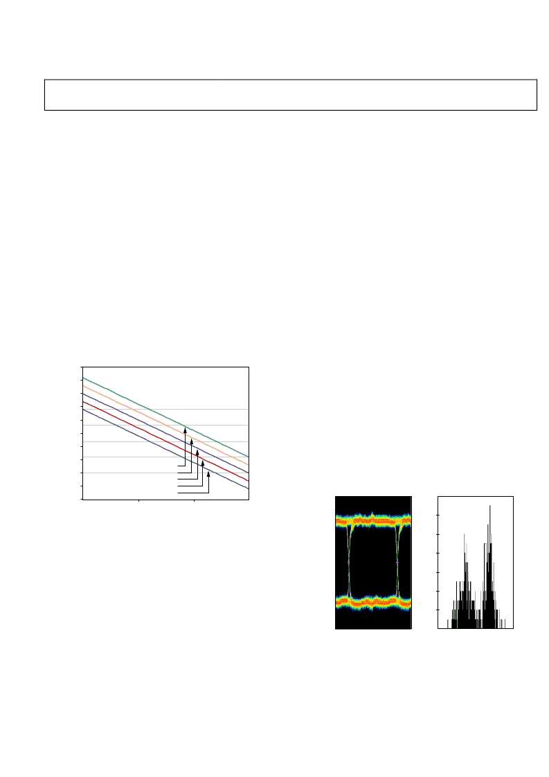
An example of the LVDS output using the ANSI standard (default)
data eye and a time interval error (TIE) jitter histogram with
trace lengths less than 24 inches on regular FR-4 material is
shown in Figure 48. Figure 49 shows an example of when the
trace lengths exceed 24 inches on regular FR-4 material. Notice
that the TIE jitter histogram reflects the decrease of the data eye
opening as the edge deviates from the ideal position. It is up to
the user to determine if the waveforms meet the timing budget
of the design when the trace lengths exceed 24 inches.
500
–500
–400
–300
–200
–100
0
100
200
300
400
–3
–2
–1
0
1
2
3
E
TIME (ns)
14
12
10
8
6
4
2
0
–40
–20
0
20
40
T
TIME (ps)
0
Figure 48. Data Eye for LVDS Outputs in ANSI Mode with Trace Lengths Less
than 24 Inches on Standard FR-4, AD9211-250
相關PDF資料 |
PDF描述 |
|---|---|
| AD9211 | 10-Bit, 170/200/250 MSPS 1.8 V A/D Converter |
| AD9211-170EB | 10-Bit, 170/200/250 MSPS 1.8 V A/D Converter |
| AD9211-200EB | 10-Bit, 170/200/250 MSPS 1.8 V A/D Converter |
| AD9211-250EB | 10-Bit, 170/200/250 MSPS 1.8 V A/D Converter |
| AD9211BCPZ-170 | 10-Bit, 170/200/250 MSPS 1.8 V A/D Converter |
相關代理商/技術參數 |
參數描述 |
|---|---|
| AD9212 | 制造商:AD 制造商全稱:Analog Devices 功能描述:Octal, 10-Bit, 40/65 MSPS Serial LVDS 1.8 V A/D Converter |
| AD9212_11 | 制造商:AD 制造商全稱:Analog Devices 功能描述:Octal, 10-Bit, 40 MSPS/65 MSPS, Serial LVDS, 1.8 V ADC |
| AD9212-65EB1 | 制造商:AD 制造商全稱:Analog Devices 功能描述:High Speed ADC USB FIFO Evaluation Kit |
| AD9212-65EBZ | 功能描述:BOARD EVALUATION FOR AD9212 RoHS:是 類別:編程器,開發系統 >> 評估板 - 模數轉換器 (ADC) 系列:- 產品培訓模塊:Obsolescence Mitigation Program 標準包裝:1 系列:- ADC 的數量:1 位數:12 采樣率(每秒):94.4k 數據接口:USB 輸入范圍:±VREF/2 在以下條件下的電源(標準):- 工作溫度:-40°C ~ 85°C 已用 IC / 零件:MAX11645 已供物品:板,軟件 |
| AD9212ABCPZ-40 | 功能描述:IC ADC 10BIT SRL 40MSPS 64LFCSP RoHS:是 類別:集成電路 (IC) >> 數據采集 - 模數轉換器 系列:- 標準包裝:1 系列:- 位數:14 采樣率(每秒):83k 數據接口:串行,并聯 轉換器數目:1 功率耗散(最大):95mW 電壓電源:雙 ± 工作溫度:0°C ~ 70°C 安裝類型:通孔 封裝/外殼:28-DIP(0.600",15.24mm) 供應商設備封裝:28-PDIP 包裝:管件 輸入數目和類型:1 個單端,雙極 |
發布緊急采購,3分鐘左右您將得到回復。