- 您現在的位置:買賣IC網 > PDF目錄373959 > AD9212 (Analog Devices, Inc.) Octal, 10-Bit, 40/65 MSPS Serial LVDS 1.8 V A/D Converter PDF資料下載
參數資料
| 型號: | AD9212 |
| 廠商: | Analog Devices, Inc. |
| 英文描述: | Octal, 10-Bit, 40/65 MSPS Serial LVDS 1.8 V A/D Converter |
| 中文描述: | 八路,10位,六十五分之四十〇 MSPS的串行LVDS 1.8弗吉尼亞州/ D轉換器 |
| 文件頁數: | 23/56頁 |
| 文件大小: | 1840K |
| 代理商: | AD9212 |
第1頁第2頁第3頁第4頁第5頁第6頁第7頁第8頁第9頁第10頁第11頁第12頁第13頁第14頁第15頁第16頁第17頁第18頁第19頁第20頁第21頁第22頁當前第23頁第24頁第25頁第26頁第27頁第28頁第29頁第30頁第31頁第32頁第33頁第34頁第35頁第36頁第37頁第38頁第39頁第40頁第41頁第42頁第43頁第44頁第45頁第46頁第47頁第48頁第49頁第50頁第51頁第52頁第53頁第54頁第55頁第56頁
AD9212
Clock Jitter Considerations
High speed, high resolution ADCs are sensitive to the quality of the
clock input. The degradation in SNR at a given input frequency
(f
A
) due only to aperture jitter (t
J
) can be calculated by
SNR degradation
= 20 × log 10 [1/2 × π ×
f
A
×
t
J
]
In this equation, the rms aperture jitter represents the root mean
square of all jitter sources, including the clock input, analog input
signal, and ADC aperture jitter specifications. IF undersampling
applications are particularly sensitive to jitter (see Figure 56).
The clock input should be treated as an analog signal in cases
where aperture jitter may affect the dynamic range of the AD9212.
Power supplies for clock drivers should be separated from the
ADC output driver supplies to avoid modulating the clock signal
with digital noise. Low jitter, crystal-controlled oscillators make
the best clock sources. If the clock is generated from another
type of source (by gating, dividing, or other methods), it should
be retimed by the original clock at the last step.
Refer to the AN-501 Application Note
and the AN-756
Application Note for more in-depth information about jitter
performance as it relates to ADCs (visit
www.analog.com
).
Rev. 0 | Page 23 of 56
1
10
100
1000
16 BITS
14 BITS
12 BITS
30
40
50
60
70
80
90
100
110
120
130
0.125ps
0.25ps
0.5ps
1.0ps
2.0ps
ANALOG INPUT FREQUENCY (MHz)
10 BITS
8 BITS
RMS CLOCK JITTER REQUIREMENT
S
0
Figure 56. Ideal SNR vs. Input Frequency and Jitter
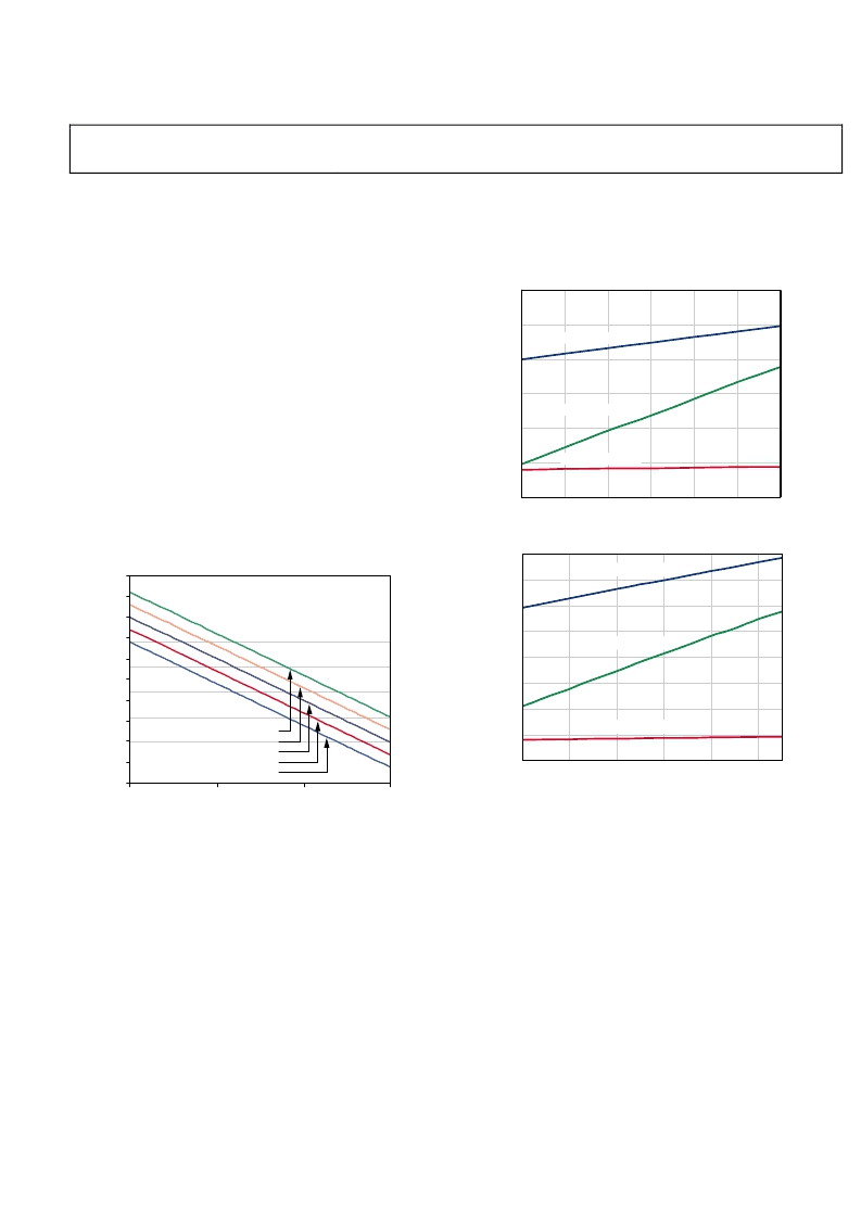
Power Dissipation and Power-Down Mode
As shown in Figure 57 and Figure 58, the power dissipated by
the AD9212 is proportional to its sample rate. The digital power
dissipation does not vary much because it is determined primarily
by the DRVDD supply and bias current of the LVDS output drivers.
0
0
0.05
0.10
0.15
0.20
0.25
0.30
10
15
20
25
30
35
40
ENCODE (MHz)
C
0.40
0.42
0.44
0.46
0.48
0.50
0.52
0.54
0.56
0.58
0.60
P
TOTAL POWER
AVDD CURRENT
DRVDD CURRENT
Figure 57. Supply Current vs. f
SAMPLE
for f
IN
= 10.3 MHz, AD9212-40
0
0
0.05
0.10
0.15
0.20
0.25
0.30
0.35
0.40
10
20
30
40
50
60
ENCODE (MHz)
C
0.50
0.55
0.60
0.65
0.70
0.75
0.80
0.85
0.90
P
TOTAL POWER
AVDD CURRENT
DRVDD CURRENT
Figure 58. Supply Current vs. f
SAMPLE
for f
IN
= 10.3 MHz, AD9212-65
相關PDF資料 |
PDF描述 |
|---|---|
| AD9212-65EBZ | Octal, 10-Bit, 40/65 MSPS Serial LVDS 1.8 V A/D Converter |
| AD9212BCPZ-40 | Octal, 10-Bit, 40/65 MSPS Serial LVDS 1.8 V A/D Converter |
| AD9212BCPZ-65 | Octal, 10-Bit, 40/65 MSPS Serial LVDS 1.8 V A/D Converter |
| AD9212BCPZRL7-40 | Octal, 10-Bit, 40/65 MSPS Serial LVDS 1.8 V A/D Converter |
| AD9212BCPZRL7-65 | Octal, 10-Bit, 40/65 MSPS Serial LVDS 1.8 V A/D Converter |
相關代理商/技術參數 |
參數描述 |
|---|---|
| AD9212_11 | 制造商:AD 制造商全稱:Analog Devices 功能描述:Octal, 10-Bit, 40 MSPS/65 MSPS, Serial LVDS, 1.8 V ADC |
| AD9212-65EB1 | 制造商:AD 制造商全稱:Analog Devices 功能描述:High Speed ADC USB FIFO Evaluation Kit |
| AD9212-65EBZ | 功能描述:BOARD EVALUATION FOR AD9212 RoHS:是 類別:編程器,開發系統 >> 評估板 - 模數轉換器 (ADC) 系列:- 產品培訓模塊:Obsolescence Mitigation Program 標準包裝:1 系列:- ADC 的數量:1 位數:12 采樣率(每秒):94.4k 數據接口:USB 輸入范圍:±VREF/2 在以下條件下的電源(標準):- 工作溫度:-40°C ~ 85°C 已用 IC / 零件:MAX11645 已供物品:板,軟件 |
| AD9212ABCPZ-40 | 功能描述:IC ADC 10BIT SRL 40MSPS 64LFCSP RoHS:是 類別:集成電路 (IC) >> 數據采集 - 模數轉換器 系列:- 標準包裝:1 系列:- 位數:14 采樣率(每秒):83k 數據接口:串行,并聯 轉換器數目:1 功率耗散(最大):95mW 電壓電源:雙 ± 工作溫度:0°C ~ 70°C 安裝類型:通孔 封裝/外殼:28-DIP(0.600",15.24mm) 供應商設備封裝:28-PDIP 包裝:管件 輸入數目和類型:1 個單端,雙極 |
| AD9212ABCPZ-65 | 功能描述:IC ADC 10BIT SRL 65MSPS 64LFCSP RoHS:是 類別:集成電路 (IC) >> 數據采集 - 模數轉換器 系列:- 標準包裝:1 系列:- 位數:14 采樣率(每秒):83k 數據接口:串行,并聯 轉換器數目:1 功率耗散(最大):95mW 電壓電源:雙 ± 工作溫度:0°C ~ 70°C 安裝類型:通孔 封裝/外殼:28-DIP(0.600",15.24mm) 供應商設備封裝:28-PDIP 包裝:管件 輸入數目和類型:1 個單端,雙極 |
發布緊急采購,3分鐘左右您將得到回復。