- 您現在的位置:買賣IC網 > PDF目錄373959 > AD9212 (Analog Devices, Inc.) Octal, 10-Bit, 40/65 MSPS Serial LVDS 1.8 V A/D Converter PDF資料下載
參數資料
| 型號: | AD9212 |
| 廠商: | Analog Devices, Inc. |
| 英文描述: | Octal, 10-Bit, 40/65 MSPS Serial LVDS 1.8 V A/D Converter |
| 中文描述: | 八路,10位,六十五分之四十〇 MSPS的串行LVDS 1.8弗吉尼亞州/ D轉換器 |
| 文件頁數: | 37/56頁 |
| 文件大小: | 1840K |
| 代理商: | AD9212 |
第1頁第2頁第3頁第4頁第5頁第6頁第7頁第8頁第9頁第10頁第11頁第12頁第13頁第14頁第15頁第16頁第17頁第18頁第19頁第20頁第21頁第22頁第23頁第24頁第25頁第26頁第27頁第28頁第29頁第30頁第31頁第32頁第33頁第34頁第35頁第36頁當前第37頁第38頁第39頁第40頁第41頁第42頁第43頁第44頁第45頁第46頁第47頁第48頁第49頁第50頁第51頁第52頁第53頁第54頁第55頁第56頁
AD9212
DEFAULT OPERATION AND JUMPER SELECTION
SETTINGS
The following is a list of the default and optional settings or
modes allowed on the AD9212 Rev. A evaluation board.
POWER: Connect the switching power supply that is
supplied in the evaluation kit between a rated 100 V ac
to 240 V ac wall outlet at 47 Hz to 63 Hz and P701.
AIN: The evaluation board is set up for a transformer-
coupled analog input with optimum 50 Ω impedance
matching out to 150 MHz (see Figure 75). For more
bandwidth response, the differential capacitor across the
analog inputs can be changed or removed. The common
mode of the analog inputs is developed from the center
tap of the transformer or AVDD_DUT/2.
Rev. 0 | Page 37 of 56
–14
–13
–12
–11
–10
–9
–8
–7
–6
–5
–4
–3
–2
–1
0
0
50
100
150
200
250
300
350
400
450
500
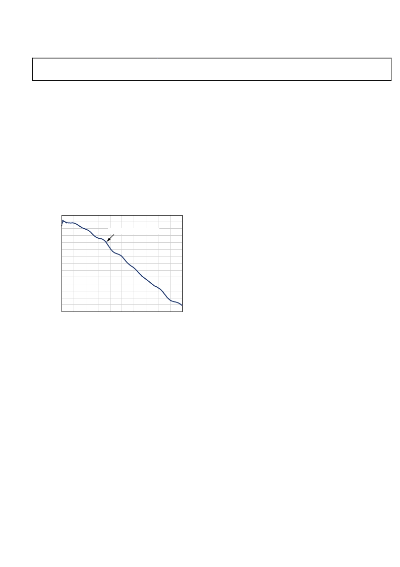
FREQUENCY (MHz)
A
–3dB CUTOFF = 186MHz
0
Figure 75. Evaluation Board Full Power Bandwidth
VREF: VREF is set to 1.0 V by tying the SENSE pin to
ground, R317. This causes the ADC to operate in 2.0 V p-p
full-scale range. A separate external reference option using
the ADR510 or ADR520 is also included on the evaluation
board. Simply populate R312 and R313 and remove C307.
Proper use of the VREF options is noted in the Voltage
Reference section.
RBIAS: RBIAS has a default setting of 10 kΩ (R301) to
ground and is used to set the ADC core bias current. To
further lower the core power (excluding the LVDS driver
supply), simply change the resistor setting. However,
performance of the ADC will degrade depending on the
resistor chosen. See RBIAS section for more information.
CLOCK: The default clock input circuitry is derived from a
simple transformer-coupled circuit using a high bandwidth
1:1 impedance ratio transformer (T401) that adds a very
low amount of jitter to the clock path. The clock input is
50 Ω terminated and ac-coupled to handle single-ended
sine wave types of inputs. The transformer converts the
single-ended input to a differential signal that is clipped
before entering the ADC clock inputs.
A differential LVPECL clock can also be used to clock the
ADC input using the AD9515 (U401). Simply populate
R406 and R407 with 0 Ω resistors and remove R215 and
R216 to disconnect the default clock path inputs. In addition,
populate C205 and C206 with a 0.1 μF capacitor and remove
C409 and C410 to disconnect the default clock path outputs.
The AD9515 has many pin-strappable options that are set
to a default working condition. Consult the AD9515 data
sheet for more information about these and other options.
If using an oscillator, two oscillator footprint options are
also available (OSC401) to check the ADC performance.
J401 gives the user flexibility in using the enable pin, which
is common on most oscillators.
PDWN: To enable the power-down feature, simply short
J301 to the on position (AVDD) on the PDWN pin.
SCLK/DTP: To enable a digital test pattern on the digital
outputs of the ADC, use J304. If J304 is tied to AVDD during
device power-up, Test Pattern 10 0000 0000 will be enabled.
See the SCLK/DTP Pin section for details.
SDIO/ODM: To enable the low power, reduced signal option
similar to the IEEE 1595.3 reduced range link LVDS output
standard, use J303. If J303 is tied to AVDD during device
power-up, it enables the LVDS outputs in a low power,
reduced signal option from the default ANSI standard.
This option changes the signal swing from 350 mV p-p to
200 mV p-p, which reduces the power of the DRVDD supply.
See the SDIO/ODM Pin section for more details.
CSB: To enable the SPI information on the SDIO and
SCLK pins that is to be processed, simply tie J302 low in
the always enable mode. To ignore the SDIO and SCLK
information, tie J302 to AVDD.
Non-SPI Mode: For users who wish to operate the DUT
without using SPI, simply remove Jumpers J302, J303, and
J304. This disconnects the CSB, SCLK/DTP, and SDIO/OMD
pins from the control bus, allowing the DUT to operate in
its simplest mode. Each of these pins has internal termination
and will float to its respective level.
D+, D: If an alternative data capture method to the setup
described in Figure 76 is used, optional receiver terminations,
R318, R320 to R328, can be installed next to the high speed
backplane connector.
相關PDF資料 |
PDF描述 |
|---|---|
| AD9212-65EBZ | Octal, 10-Bit, 40/65 MSPS Serial LVDS 1.8 V A/D Converter |
| AD9212BCPZ-40 | Octal, 10-Bit, 40/65 MSPS Serial LVDS 1.8 V A/D Converter |
| AD9212BCPZ-65 | Octal, 10-Bit, 40/65 MSPS Serial LVDS 1.8 V A/D Converter |
| AD9212BCPZRL7-40 | Octal, 10-Bit, 40/65 MSPS Serial LVDS 1.8 V A/D Converter |
| AD9212BCPZRL7-65 | Octal, 10-Bit, 40/65 MSPS Serial LVDS 1.8 V A/D Converter |
相關代理商/技術參數 |
參數描述 |
|---|---|
| AD9212_11 | 制造商:AD 制造商全稱:Analog Devices 功能描述:Octal, 10-Bit, 40 MSPS/65 MSPS, Serial LVDS, 1.8 V ADC |
| AD9212-65EB1 | 制造商:AD 制造商全稱:Analog Devices 功能描述:High Speed ADC USB FIFO Evaluation Kit |
| AD9212-65EBZ | 功能描述:BOARD EVALUATION FOR AD9212 RoHS:是 類別:編程器,開發系統 >> 評估板 - 模數轉換器 (ADC) 系列:- 產品培訓模塊:Obsolescence Mitigation Program 標準包裝:1 系列:- ADC 的數量:1 位數:12 采樣率(每秒):94.4k 數據接口:USB 輸入范圍:±VREF/2 在以下條件下的電源(標準):- 工作溫度:-40°C ~ 85°C 已用 IC / 零件:MAX11645 已供物品:板,軟件 |
| AD9212ABCPZ-40 | 功能描述:IC ADC 10BIT SRL 40MSPS 64LFCSP RoHS:是 類別:集成電路 (IC) >> 數據采集 - 模數轉換器 系列:- 標準包裝:1 系列:- 位數:14 采樣率(每秒):83k 數據接口:串行,并聯 轉換器數目:1 功率耗散(最大):95mW 電壓電源:雙 ± 工作溫度:0°C ~ 70°C 安裝類型:通孔 封裝/外殼:28-DIP(0.600",15.24mm) 供應商設備封裝:28-PDIP 包裝:管件 輸入數目和類型:1 個單端,雙極 |
| AD9212ABCPZ-65 | 功能描述:IC ADC 10BIT SRL 65MSPS 64LFCSP RoHS:是 類別:集成電路 (IC) >> 數據采集 - 模數轉換器 系列:- 標準包裝:1 系列:- 位數:14 采樣率(每秒):83k 數據接口:串行,并聯 轉換器數目:1 功率耗散(最大):95mW 電壓電源:雙 ± 工作溫度:0°C ~ 70°C 安裝類型:通孔 封裝/外殼:28-DIP(0.600",15.24mm) 供應商設備封裝:28-PDIP 包裝:管件 輸入數目和類型:1 個單端,雙極 |
發布緊急采購,3分鐘左右您將得到回復。