- 您現(xiàn)在的位置:買賣IC網(wǎng) > PDF目錄373959 > AD9214-105PCB (Analog Devices, Inc.) 10-Bit, 65/80/105 MSPS 3 V A/D Converter PDF資料下載
參數(shù)資料
| 型號(hào): | AD9214-105PCB |
| 廠商: | Analog Devices, Inc. |
| 元件分類: | ADC |
| 英文描述: | 10-Bit, 65/80/105 MSPS 3 V A/D Converter |
| 中文描述: | 10位,65/80/105MSPS的3V A/D轉(zhuǎn)換器 |
| 文件頁數(shù): | 12/20頁 |
| 文件大小: | 447K |
| 代理商: | AD9214-105PCB |
REV. D
AD9214
–12–
THEORY OF OPERATION
The AD9214 architecture is a bit-per-stage pipeline converter
utilizing switch capacitor techniques. These stages determine
the 7 MSBs and drive a 3-bit flash. Each stage provides suffi-
cient overlap and error correction allowing optimization of
comparator accuracy. The input buffer is differential and both
inputs are internally biased. This allows the most flexible use of
ac or dc and differential or single-ended input modes. The out-
put staging block aligns the data, carries out the error correction
and feeds the data to output buffers. The output buffers are
powered from a separate supply, allowing support of different
logic families. During power-down, the outputs go to a high
impedance state.
APPLYING THE AD9214
Encoding the AD9214
Any high-speed A/D converter is extremely sensitive to the
quality of the sampling clock provided by the user. A Track/
Hold circuit is essentially a mixer. Any noise, distortion, or
timing jitter on the clock will be combined with the desired
signal at the A/D output. For that reason, considerable care has
been taken in the design of the ENCODE input of the AD9214,
and the user is advised to give commensurate thought to the clock
source. The ENCODE input is fully TTL/CMOS compatible, and
should normally be driven directly from a low jitter, crystal-
controlled TTL/CMOS oscillator.
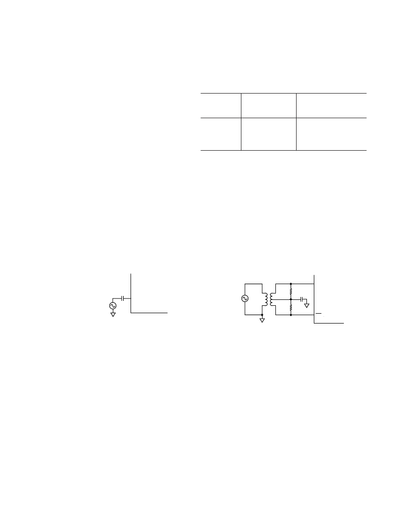
The ENCODE input is internally biased, allowing the user to
ac-couple in the clock signal. The cleanest clock source is often
a crystal oscillator producing a pure sine wave. Figure 7 illustrates
ac coupling such a source to the ENCODE input.
ENCODE
LOW JITTER CRYSTAL SINE OR
PULSE SOURCE 1V p-p
AD9214
Figure 7. AC-Coupled Encode Circuit
Reference Circuit
The reference circuit of the AD9214 is configured by REFSENSE
(Pin 3). By externally connecting REFSENSE to AGND, the
ADC is configured to use the internal reference (~1.25 V), and
the REF pin connection (Pin 4) is configured as an output for
the internal reference voltage.
If REFSENSE is externally connected to AV
DD
, the ADC is
configured to use an external reference. In this mode, the REF
pin is configured as a reference input, and must be driven by an
external 1.25 V reference.
In either configuration, the analog input voltage range (either
1 V p-p or 2 V p-p as determined by DFS/Gain) will track the
reference voltage linearly, and an external bypass capacitor should
be connected between REF and AGND to reduce noise on the
reference. In practice, no appreciable degradation in performance
occurs when an external reference is adjusted
±
5%.
DFS/GAIN
The DFS/GAIN (Data Format Select/Gain) input (Pin 2)
controls both the output data format and gain (analog input volt-
age range) of the ADC. The table below describes its operation.
Table I. Data Format and Gain Configuration
External
DFS/GAIN
Connection
Differential
Analog Input
Voltage Range
Output Data Format
AGND
AV
DD
REF
Floating
1 V p-p
1 V p-p
2 V p-p
2 V p-p
Offset Binary
Two
’
s Complement
Two
’
s Complement
Offset Binary
Driving the Analog Inputs
The analog input to the AD9214 is a differential buffer. As
shown in the equivalent circuits, each of the differential inputs is
internally dc biased at ~AV
DD
/3 to allow ac-coupling of the
analog input signal. The analog signal may be dc-coupled as
well. In this case, the dc load will be equivalent to ~10 k
to
AV
DD
/3, and the dc common-mode level of the analog signals
should be within the range of AV
DD
/3
±
200 mV. For best dynamic
performance, impedances at A
IN
and
A
IN
should match.
Driving the analog input differentially optimizes ac performance,
minimizing even order harmonics and taking advantage of
common-mode rejection of noise. A differential signal may be
transformer-coupled, as illustrated in Figure 8, or driven from a
high-performance differential amplifier such as the AD8138
illustrated in Figure 9.
A
IN
A
IN
0.1 F
25
25
1:1
50
ANALOG
SIGNAL
SOURCE
AD9214
Figure 8. Single-Ended-to-Differential Conversion Using
a Transformer
Special care was taken in the design of the analog input section
of the AD9214 to prevent damage and corruption of data when
the input is overdriven. The optimal input range is 1.0 V p-p, but
the AD9214 can support a 2.0 V p-p input range with some degra-
dation in performance (see DFS/GAIN pin description above).
相關(guān)PDF資料 |
PDF描述 |
|---|---|
| AD9214-65PCB | 10-Bit, 65/80/105 MSPS 3 V A/D Converter |
| AD9214BRS-105 | 10-Bit, 65/80/105 MSPS 3 V A/D Converter |
| AD9214BRS-65 | 10-Bit, 65/80/105 MSPS 3 V A/D Converter |
| AD9214BRS-80 | TV07RW21-35SA W/ PC CONTACTS |
| AD9215BCPZ-80 | 10-Bit, 65/80/105 MSPS, 3V A/D Converter |
相關(guān)代理商/技術(shù)參數(shù) |
參數(shù)描述 |
|---|---|
| AD9214-65PCB | 制造商:Analog Devices 功能描述:10 BIT 65 MSPS A/D CONVERTER EVAL BOARD - Bulk |
| AD9214BRS-105 | 功能描述:IC ADC 10BIT 105MSPS 3V 28-SSOP RoHS:否 類別:集成電路 (IC) >> 數(shù)據(jù)采集 - 模數(shù)轉(zhuǎn)換器 系列:- 產(chǎn)品培訓(xùn)模塊:Lead (SnPb) Finish for COTS Obsolescence Mitigation Program 標(biāo)準(zhǔn)包裝:2,500 系列:- 位數(shù):12 采樣率(每秒):3M 數(shù)據(jù)接口:- 轉(zhuǎn)換器數(shù)目:- 功率耗散(最大):- 電壓電源:- 工作溫度:- 安裝類型:表面貼裝 封裝/外殼:SOT-23-6 供應(yīng)商設(shè)備封裝:SOT-23-6 包裝:帶卷 (TR) 輸入數(shù)目和類型:- |
| AD9214BRS-65 | 功能描述:IC ADC 10BIT 65MSPS 28-SSOP RoHS:否 類別:集成電路 (IC) >> 數(shù)據(jù)采集 - 模數(shù)轉(zhuǎn)換器 系列:- 產(chǎn)品培訓(xùn)模塊:Lead (SnPb) Finish for COTS Obsolescence Mitigation Program 標(biāo)準(zhǔn)包裝:2,500 系列:- 位數(shù):12 采樣率(每秒):3M 數(shù)據(jù)接口:- 轉(zhuǎn)換器數(shù)目:- 功率耗散(最大):- 電壓電源:- 工作溫度:- 安裝類型:表面貼裝 封裝/外殼:SOT-23-6 供應(yīng)商設(shè)備封裝:SOT-23-6 包裝:帶卷 (TR) 輸入數(shù)目和類型:- |
| AD9214BRS-80 | 功能描述:IC ADC 10BIT 80MSPS 28-SSOP RoHS:否 類別:集成電路 (IC) >> 數(shù)據(jù)采集 - 模數(shù)轉(zhuǎn)換器 系列:- 產(chǎn)品培訓(xùn)模塊:Lead (SnPb) Finish for COTS Obsolescence Mitigation Program 標(biāo)準(zhǔn)包裝:2,500 系列:- 位數(shù):12 采樣率(每秒):3M 數(shù)據(jù)接口:- 轉(zhuǎn)換器數(shù)目:- 功率耗散(最大):- 電壓電源:- 工作溫度:- 安裝類型:表面貼裝 封裝/外殼:SOT-23-6 供應(yīng)商設(shè)備封裝:SOT-23-6 包裝:帶卷 (TR) 輸入數(shù)目和類型:- |
| AD9214BRSRL105 | 制造商:AD 功能描述:New |
發(fā)布緊急采購,3分鐘左右您將得到回復(fù)。