- 您現在的位置:買賣IC網 > PDF目錄373960 > AD9224ARS (ANALOG DEVICES INC) Complete 12-Bit 40 MSPS Monolithic A/D Converter PDF資料下載
參數資料
| 型號: | AD9224ARS |
| 廠商: | ANALOG DEVICES INC |
| 元件分類: | ADC |
| 英文描述: | Complete 12-Bit 40 MSPS Monolithic A/D Converter |
| 中文描述: | 1-CH 12-BIT PROPRIETARY METHOD ADC, PARALLEL ACCESS, PDSO28 |
| 封裝: | SSOP-28 |
| 文件頁數: | 16/24頁 |
| 文件大小: | 309K |
| 代理商: | AD9224ARS |
AD9224
–16–
REV. A
REFERENCE CONFIGURATIONS
The figures associated with this section on internal and external
reference operation do not show recommended matching series
resistors for VINA and VINB for the purpose of simplicity.
Please refer to the Driving the Analog Inputs section for a dis-
cussion of this topic. Also, the figures do not show the decou-
pling network associated with the CAPT and CAPB pins.
Please refer to the Reference Operation section for a discussion
of the internal reference circuitry and the recommended decou-
pling network shown in Figure 17.
USING THE INTERNAL REFERENCE
Single-Ended Input with 0 to 2
3
VREF Range
Figure 26a shows how to connect the AD9224 for a 0 V to 2 V
or 0 V to 4 V input range via pin strapping the SENSE pin. An
intermediate input range of 0 to 2
×
VREF can be established
using the resistor programmable configuration in Figure 28.
In either case, both the midscale voltage and input span are
directly dependent on the value of VREF. More specifically, the
midscale voltage is equal to VREF while the input span is equal
to 2
×
VREF. Thus, the valid input range extends from 0 to 2
×
VREF. When VINA is
≤
0 V, the digital output will be 000 Hex;
when VINA is
≥
2
×
VREF, the digital output will be FFF Hex.
Shorting the VREF pin directly to the SENSE pin places the
internal reference amplifier in unity-gain mode and the resultant
VREF output is 1 V. Therefore, the valid input range is 0 V to
2 V. However, shorting the SENSE pin directly to the REFCOM
pin configures the internal reference amplifier for a gain of 2.0
and the resultant VREF output is 2.0 V. Thus, the valid input
range becomes 0 V to 4 V. The VREF pin should be bypassed to
the REFCOM pin with a 10
μ
F tantalum capacitor in parallel
with a low-inductance 0.1
μ
F ceramic capacitor.
10
m
F
VINA
VREF
AD9224
0.1
m
F
VINB
2
3
VREF
0V
SHORT FOR 0V TO 2V
INPUT SPAN
SENSE
SHORT FOR 0V TO 4V
INPUT SPAN
REFCOM
Figure 26a. Internal Reference—2 V p-p Input Span,
V
CM
= 1 V, or 4 V p-p Input Span
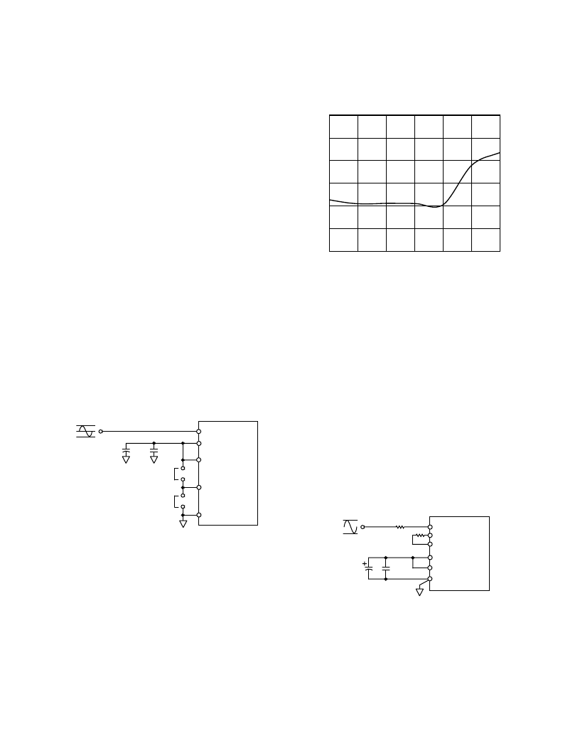
Figure 26b illustrates the relation between reference voltage and
THD. Note that optimal performance occurs when the refer-
ence voltage is set to 1.5 V (input span = 3 V).
REFERENCE VOLTAGE – V
–60
–65
–80
1.0
T
1.2
1.4
1.6
1.8
2.0
2.2
–70
–75
–85
–90
Figure 26b. THD vs. Reference Voltage, F
S
= 40 MHz,
F
IN
= 10 MHz (Differential)
Figure 27 shows the single-ended configuration that gives good
dynamic performance (SINAD, SFDR). To optimize dynamic
specifications, center the common-mode voltage of the analog
input at approximately by 2.5 V by connecting VINB to a low
impedance 2.5 V source. As described above, shorting the
VREF pin directly to the SENSE pin results in a 1 V reference
voltage and a 2 V p-p input span. The valid range for input
signals is 1.5 V to 3.5 V. The VREF pin should be bypassed to
the REFCOM pin with a 10
μ
F tantalum capacitor in parallel
with a low-inductance 0.1
μ
F ceramic capacitor.
This reference configuration could also be used for a differential
input in which VINA and VINB are driven via a transformer as
shown in Figure 24. In this case, the common-mode voltage,
V
CM
, is set at midsupply by connecting the transformer’s center
tap to CML of the AD9224. VREF can be configured for 1.0 V or
2.0 V by connecting SENSE to either VREF or REFCOM re-
spectively. Note that the valid input range for each of the
differential inputs is one half of the single-ended input and thus
becomes V
CM
– VREF/2 to V
CM
+ VREF/2.
1V
0.1
m
F
10
m
F
VINA
VCM
VINB
VREF
SENSE
REFCOM
AD9224
3.5V
1.5V
Figure 27. Internal Reference—2 V p-p Input Span,
V
CM
= 2.5 V
相關PDF資料 |
PDF描述 |
|---|---|
| AD9224 | Complete 12-Bit 40 MSPS Monolithic A/D Converter |
| AD9224-EB | Complete 12-Bit 40 MSPS Monolithic A/D Converter |
| AD9225 | Complete 12-Bit, 25 MSPS Monolithic A/D Converter |
| AD9225-EB | Complete 12-Bit, 25 MSPS Monolithic A/D Converter |
| AD9225AR | Complete 12-Bit, 25 MSPS Monolithic A/D Converter |
相關代理商/技術參數 |
參數描述 |
|---|---|
| AD9224ARSZ | 功能描述:IC ADC 12BIT 40MSPS 28-SSOP RoHS:是 類別:集成電路 (IC) >> 數據采集 - 模數轉換器 系列:- 標準包裝:1 系列:microPOWER™ 位數:8 采樣率(每秒):1M 數據接口:串行,SPI? 轉換器數目:1 功率耗散(最大):- 電壓電源:模擬和數字 工作溫度:-40°C ~ 125°C 安裝類型:表面貼裝 封裝/外殼:24-VFQFN 裸露焊盤 供應商設備封裝:24-VQFN 裸露焊盤(4x4) 包裝:Digi-Reel® 輸入數目和類型:8 個單端,單極 產品目錄頁面:892 (CN2011-ZH PDF) 其它名稱:296-25851-6 |
| AD9224ARSZRL | 功能描述:IC ADC 12BIT 40MSPS 28SSOP RoHS:是 類別:集成電路 (IC) >> 數據采集 - 模數轉換器 系列:- 標準包裝:1,000 系列:- 位數:12 采樣率(每秒):300k 數據接口:并聯 轉換器數目:1 功率耗散(最大):75mW 電壓電源:單電源 工作溫度:0°C ~ 70°C 安裝類型:表面貼裝 封裝/外殼:24-SOIC(0.295",7.50mm 寬) 供應商設備封裝:24-SOIC 包裝:帶卷 (TR) 輸入數目和類型:1 個單端,單極;1 個單端,雙極 |
| AD9224-EB | 制造商:Analog Devices 功能描述:Evaluation Kit For Complete 12-Bit, 40 MSPS Monolithic A/D Converter 制造商:Analog Devices 功能描述:EVAL KIT FOR COMPLETE 12-BIT, 40 MSPS MONOLITHIC A/D CNVRTR - Bulk 制造商:Rochester Electronics LLC 功能描述:12-BIT 40 MSPS MONOLITHIC A/D CONVERTER - Bulk |
| AD9224JR | 制造商:未知廠家 制造商全稱:未知廠家 功能描述:Analog-to-Digital Converter, 12-Bit |
| AD9224JRS | 制造商:未知廠家 制造商全稱:未知廠家 功能描述:Analog-to-Digital Converter, 12-Bit |
發布緊急采購,3分鐘左右您將得到回復。